

Light emitting diode device
a technology of light-emitting diodes and diodes, which is applied in the direction of static indicating devices, thermoelectric devices, instruments, etc., can solve the problems of device not being able to drive with direct current at a low voltage, reducing the effective luminance as an average luminance for a predetermined time, and difficult miniaturizing the apparatus and improving the arrangement precision
- Summary
- Abstract
- Description
- Claims
- Application Information
AI Technical Summary
Problems solved by technology
Method used
Image

Examples
first embodiment
FIG. 3 is a drawing showing an equivalent circuit of a single pixel in a light emitting diode device of the present invention. The circuit shown in FIG. 3 comprises a diode (writing diode) 1 which constitutes the pixel, and an organic light emitting diode 4 serving as a light emitting portion and having an equivalent capacity component 4-C, an equivalent resistance component 4-R and an equivalent diode component 4-D. The circuit also comprises an electrode Pd connected to the anode of the writing diode 1, and an electrode Pled connected to the cathode of the organic light emitting diode 4. A data signal is applied to the electrode Pd, and a selection signal is applied to the electrode Pled.
The circuit is operated as described below.
When the selection signal applied to the electrode Pled is brought to a selection state (low-potential state), the potential of the electrode Pled decreases. As a result, a forward voltage higher than the threshold voltage is applied to the writing diode ...
second embodiment
The equivalent circuits of a light emitting diode device of this embodiment are the same as the first embodiment.
FIG. 12 is a schematic sectional view showing the construction of the organic light emitting diode device of this embodiment.
Referring to FIG. 12, each of pixels comprises a diode (writing diode) 1, an organic light emitting diode 4 serving as a light emitting portion, and a substrate 100.
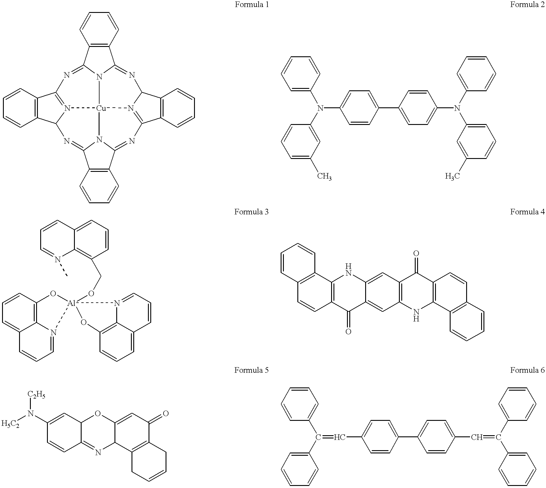
The writing diode 1 comprises a transparent electrode 101 serving as an anode and made of indium / tin oxide (ITO), a hole injection / transport layer 102 made of copper phthalocyanine (Formula 1), and a cathode 106 made of Al.
The organic light emitting diode 4 comprises a transparent electrode 401 serving as an anode and made of indium / tin oxide (ITO), a hole injection layer 402 made of copper phthalocyanine (Formula 1), a hole transport layer 403 made of aromatic diamine (Formula 2), an electron transport layer 404 made of tris(8-quinolinolato)aluminum complex (Formula 3), an electron inje...
third embodiment
The equivalent circuits of a light emitting diode device of this embodiment are the same as the first embodiment.
FIG. 15 is a schematic sectional view showing the construction of the organic light emitting diode device of this embodiment.
Referring to FIG. 15, each of pixels comprises a diode (writing diode) 1, an organic light emitting diode 4 serving as a light emitting portion, and a substrate 100.
The writing diode 1 comprises a transparent electrode 101 serving as an anode and made of indium / tin oxide (ITO), an electron transport layer 104 made of tris(8-quinolinolato)aluminum complex (Formula 3), an electron injection layer 105 made of LiF, and a cathode 106 made of Al.
The organic light emitting diode 4 comprises a transparent electrode 401 serving as an anode and made of indium / tin oxide (ITO), a hole injection layer 402 made of copper phthalocyanine (Formula 1), a hole transport layer 403 made of aromatic diamine (Formula 2), an electron transport layer 404 made of tris(8-quin...
PUM
 Abstract
Description
Claims
Application Information