Circuit manufacturing using etched tri-metal media

a tri-metal and metal multilayer technology, applied in the direction of printed circuit manufacturing, printed circuit aspects, cable/conductor manufacturing, etc., can solve the problems of insufficient bonding between metal multilayer and semiconductor substrate constituting an electrode pattern, damage to circuitry elements, and improper methods

Inactive Publication Date: 2002-04-02
BMC INDS
View PDF23 Cites 86 Cited by
  • Summary
  • Abstract
  • Description
  • Claims
  • Application Information

AI Technical Summary

Problems solved by technology

For this reason, this method is inappropriate for forming a micropattern such as a gate electrode.
However, the metal film formed by this method was formed by CVD (Chemical Vapor Deposition) at a low temperature because of a resist film.
For this reason, bonding between a metal multilayer and a semiconductor substrate constituting an electrode pattern was inadequate.
However, each such different system requires fundamental investigation of the properties and the processing necessities.
If the change in relative position between the two layers creates an internal stress (e.g., when an elastically stressed or stretched layer is laminated to an unstressed or unstretched layer), release of the externally applied tension after the layers have been laminated or otherwise joined will leave the stress between the layers within the finished article, and there could be a shearing stress within the article of sufficient strength to damage elements of the circuitry, particularly smaller, fragile elements of the circuitry, such as air bridges, or create alignment issues.
The manufacture of circuit boards has become a highly competitive field, with circuit boards being needed in essentially all modern electrical appliances and games, yet with their individual design having to be tailored for each field of use, their production having to be rapid and cost efficient, the volume capacity being extremely large, and the requirements for quality being absolute since failure of the circuitry will render each product useless.
This could prove difficult, however, as most commercial photoresists are removed when exposed to etchants that have a pH in excess of 10.5, that are used to etch the aluminum layer.
Uneven aluminum thickness or non-uniform etching of the copper or aluminum can result in undesired aluminum features remaining, which could result in electrical shorts.
Failure to control etch temperature can damage both the circuit being etched and the equipment which contains the etchant.
Some of the oxidizers that enhance the performance of the high pH etch system, for example sodium nitrate and especially sodium bromate, are both expensive and environmentally unfriendly.
Although by controlling the flow rate of the curable polymer system under the bridge, some stress forces can be reduced, this might require extremely slow production rates for higher molecular weight / higher viscosity compositions, and is not preferred.
1) Flowing under and over air bridges without bending or breaking them
2) Creating electrical termination pads that are completely surrounded, but 10 free of `ink`
3) Protecting the underlying circuit from corrosion, abrasion, vibration and physical damage
4) Producing multi-layer ETM on an inline coil process gives process economy, but introduces a difficult problem of precision alignment of 3 moving coils. We describe a system including accumulators and coil grippers or sprockets, which permit the precision positioning of the 3 layers with no relative motion. It is then possible to join them in a nip, hot roll lamination process.
The etched tri-metal circuit may be relatively fragile, depending upon the thickness of the various elements and layers, the dimensions of the circuit elements themselves, and the amount of additional structural support provided for the elements (e.g., the polymeric support for air bridges described above).
The etching of the central aluminum core layer from a Cu / Al / Cu structure can result in oxidation of the copper circuits, which may or may not have to be cleaned away.
The precision alignment and superposition of material from 3 separate, moving coils is difficult.
The peroxy-sulfuric system, which etches copper in the presence of aluminum, gives a poor profile.
Failure of a current would indicate lack of alignment.

Method used


Image

  • Circuit manufacturing using etched tri-metal media
  • Circuit manufacturing using etched tri-metal media
  • Circuit manufacturing using etched tri-metal media

Examples


Embodiment Construction

The following non-limiting example is provided to give an example of a typical process according to the present invention to support rather than limit the practice of the present invention.

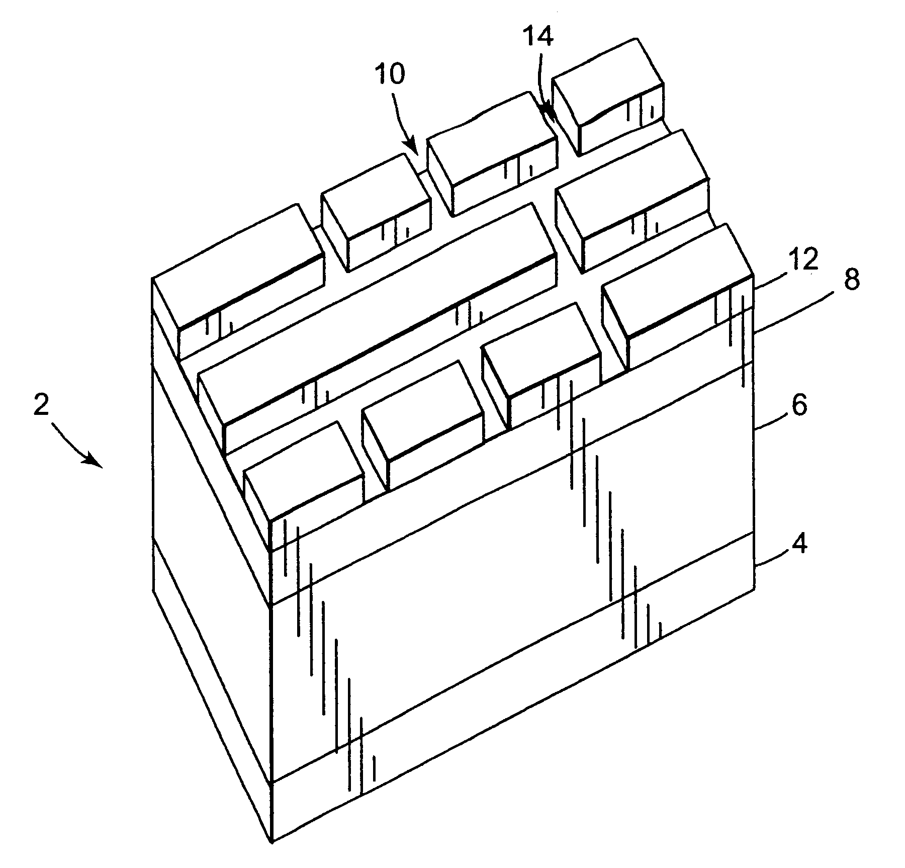
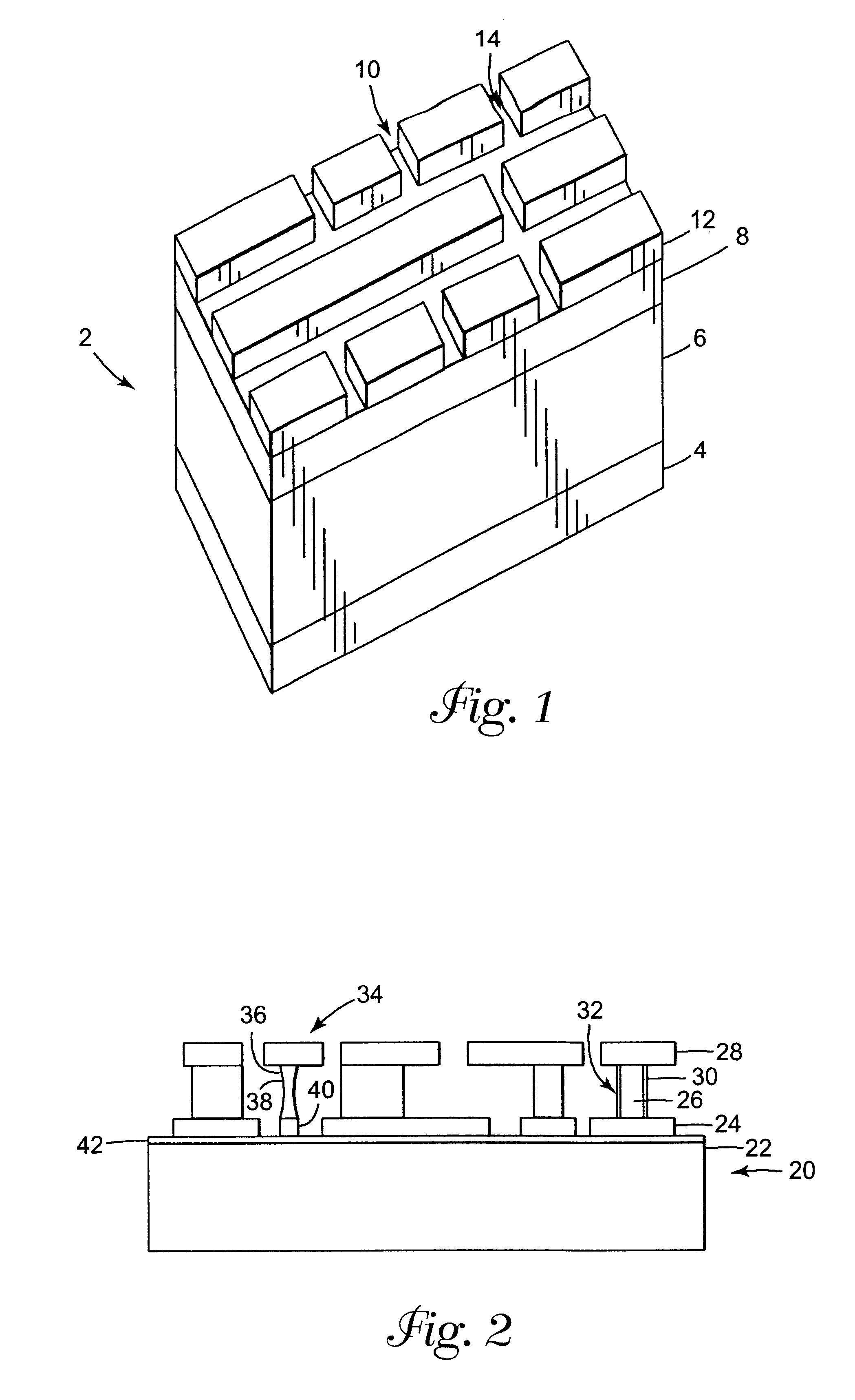
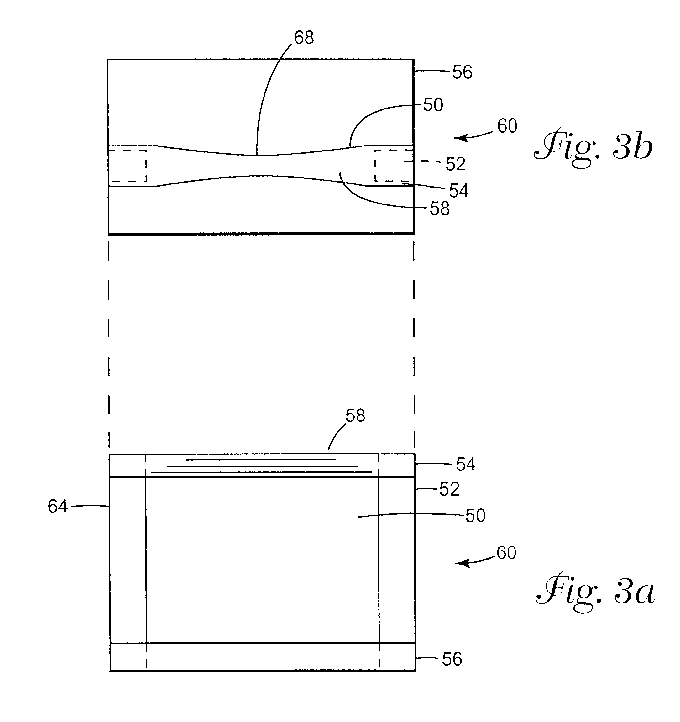
A cleaned and degreased tri-metal subelement comprising 2 mil copper / 6 mil aluminum / 2 mil copper (in a clad system) was coated with a photoresist (a commercial dry-film negative-acting photoresist from Shipley, Dynachem or Morton 5032, 1.3 mil) and the resist was imagewise exposed with ultraviolet radiation (in a pattern of an electronic circuit, including preliminary patterns for at least one air bridge). The exposed resist was developed in sodium carbonate solution removing unexposed resist. A copper etchant comprising cupric chloride was used on the imaged surface, etching the copper down to the aluminum layer. The etch of the copper layer should preferably just barely engage, expose, or approach the aluminum layer when a strong etch solution (such as cupric chloride and oxidizing agent) is use...


PUM

PropertyMeasurementUnit
elastic elongationaaaaaaaaaa
thicknessaaaaaaaaaa
thicknessaaaaaaaaaa

Abstract

A process for the formation of an article having multiple electrical circuits comprises:providing a first sub-element comprising in sequence a first metal layer of copper in electrical contact with a second metal layer of aluminum in electrical contact with a third metal layer of copper;etching an electrical circuit design in the first metal layer and in a separate etch step, etching away at least 10%, but less than 100% of the second metal layer to provide electrical connections between the first metal layer and the third metal layer;etching an electrical circuit design into the third metal layer;adhering an etched surface comprising the circuit design of the first or third metal layer to a first surface of a support layer to form a circuit board.The process may etch the first and third metal layers simultaneously or sequentially. After adhering an etched surface comprising the circuit design of the first or third metal layer to a support layer to form a circuit board, an additional step may be performed, which additional step is selected from the group consisting of;a) adhering an etched surface of a second tri-metal subelement to a second surface of the support layer andb) adhering a second support layer to said third or first metal layer, respectively, and adhering an etched surface of a second tri-metal subelement to the second support layer.

Description

1. Field of the InventionThe invention relates to articles formed from multiple metal layers used in electronic devices, and more particularly, to multiple metal layers attached to substrates to provide circuitry or circuit boards. The invention is especially advantageous when applied to manufacturing processes for thin circuit boards, particularly circuit boards with physically durable structures, including air bridges.2. Background of the ArtA technique for forming a tri-layer metal structure is described in U.S. Pat. No. 5,428,250 to Ikeda et al. The tri-layer metal structure is formed on a glass substrate. The first layer is a Ta--M--N film, the second layer is a Ta film and the third (top) layer is a Ta--M--N film, where M is at least one atom selected from the group consisting of Molybdenum, Niobium, and Tungsten.U.S. Pat. No. 5,153,754 to Whetten described a tri-layer metal structure formed on an LCD substrate where the first layer is a titanium (Ti) film, the second layer is...

Claims


Application Information

Patent Timeline
Patent Type & Authority Patents(United States)
IPC IPC(8): C23F1/36C23F1/02C23F1/44C23F1/10H01L21/02H01L21/3213H05K3/06H05K3/46
CPCH05K3/067C23F1/02C23F1/36C23F1/44H01L21/32134H05K3/4685H05K2201/0338H05K2203/0361H05K2203/0384H05K3/061H05K2203/1476
Inventor WHITEHURST, DONALD A.MATTSON, DENNIS D.WYATT, PAUL D.RING, CHARLESDUFRESNE, MICHAEL J.BRENES, JOSE F.FINGER, BRUCE A.ZEIPELT, DAVID R.
Owner BMC INDS
Why Eureka
Try Eureka