Self-aligned double-gate MOSFET by selective epitaxy and silicon wafer bonding techniques

a selective epitaxy and silicon wafer bonding technology, applied in the field of double-gate mosfets, can solve the problems of difficult to form thin vertical pillars (e.g., 10 nm) that are free of reactive ion etching damage, and difficult to keep the top and bottom gate oxides at the same thickness

Inactive Publication Date: 2002-04-02
IBM CORP
View PDF9 Cites 177 Cited by
  • Summary
  • Abstract
  • Description
  • Claims
  • Application Information

AI Technical Summary

Problems solved by technology

However there is no conventional method of making a double-gate MOSFET structure which has both the top and bottom gate self-aligned to the channel region.
However, with this method, it is difficult to form thin vertical pillars (e.g., 10 nm) that are free of reactive ion etching (RIE) damage and to maintain good thickness control.
However, with this method, it is difficult to keep the top and bottom gate oxides at the same thickness and to align the gates with each other.
However, this method also suffers silicon thickness control problems and gate alignment problems.

Method used


Image

  • Self-aligned double-gate MOSFET by selective epitaxy and silicon wafer bonding techniques
  • Self-aligned double-gate MOSFET by selective epitaxy and silicon wafer bonding techniques
  • Self-aligned double-gate MOSFET by selective epitaxy and silicon wafer bonding techniques

Examples


Embodiment Construction

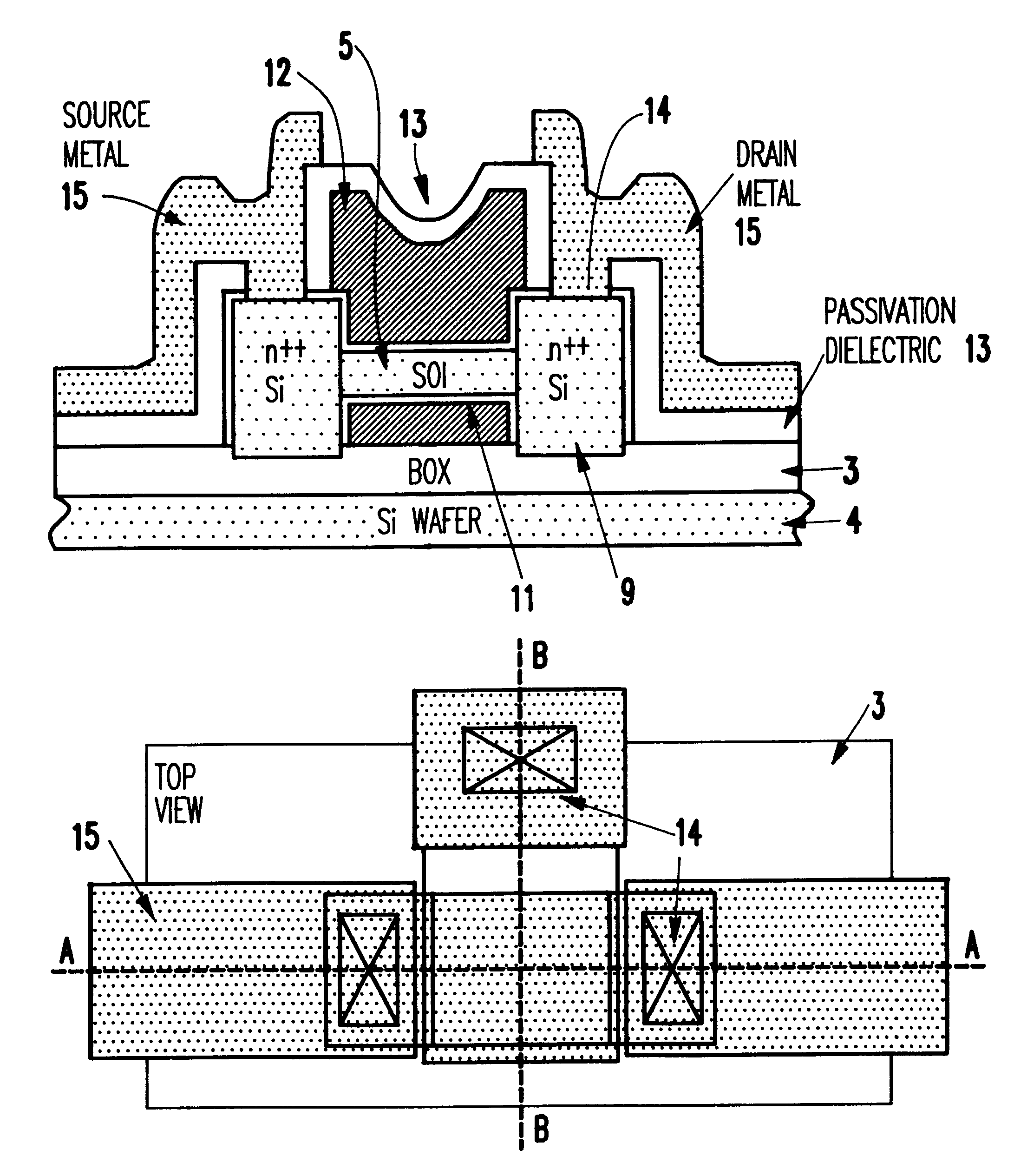
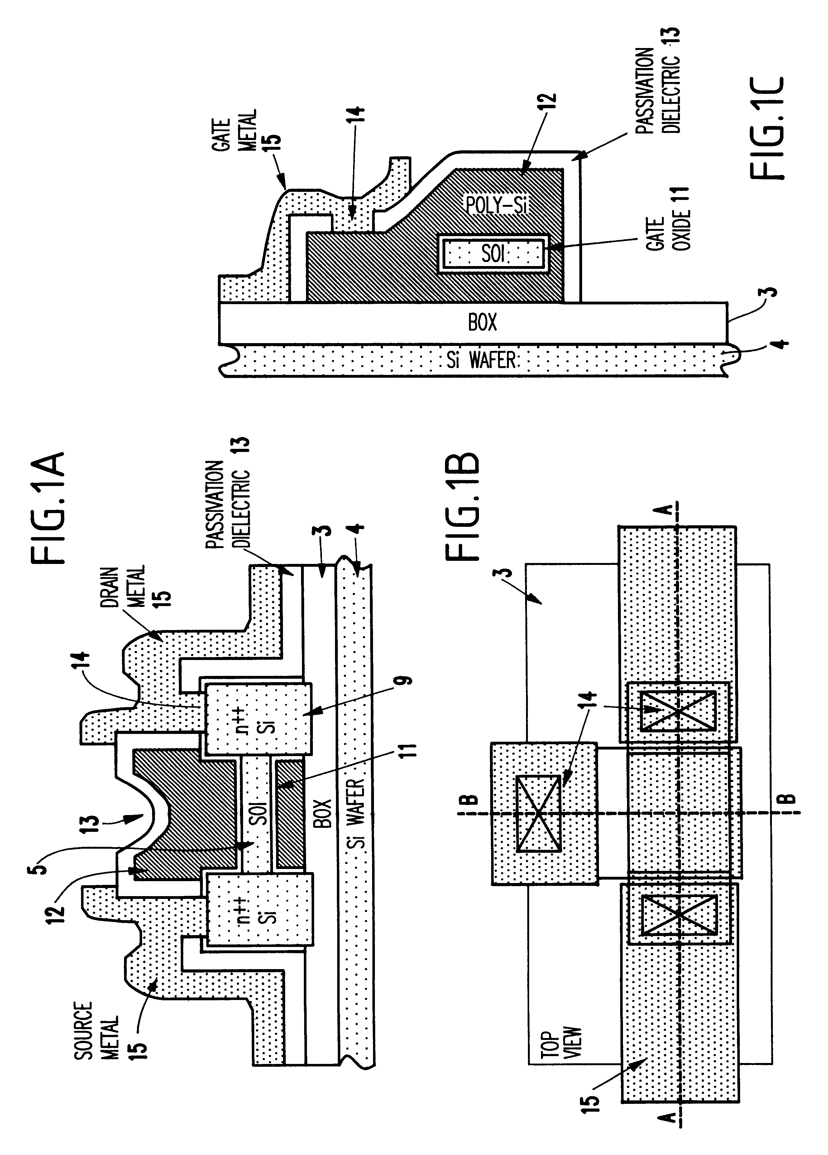
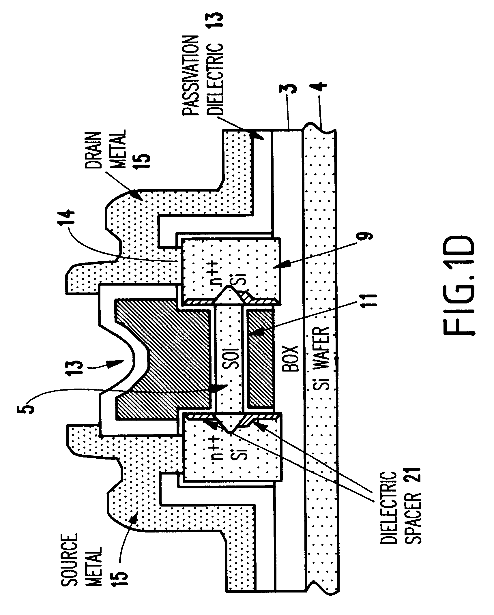
Referring now to the drawings, and more particularly to FIGS. 1A-1D, the inventive structure is illustrated. More specifically, the inventive structure includes a substrate 4, such as a silicon wafer, an insulator 3, source and drain regions 9, source, drain and gate contacts 15, contact opening 14, double-gate 12, a passivation dielectric 13, a channel region 5, an insulator and a thin gate oxide 11. FIG. 1B illustrates a top view of the inventive structure. FIG. 1A illustrates a cross-sectional view drawn along line A--A in FIG. 1B and FIG. 1C is a cross-sectional view of the structure along line B--B in FIG. 1B. FIG. 1D illustrates an alternative embodiment that includes a dielectric spacer 21, which is discussed in greater detail below with respect to FIGS. 6A-6B

A preferred method of forming the foregoing structure is discussed below with respect to FIGS. 2A-2BB. Referring now to FIG. 2A, a substrate 5 and an insulator 1 are formed using conventional manufacturing and deposition...


PUM


Abstract

A structure and a method of manufacturing a double-gate metal oxide semiconductor transistor includes forming a laminated structure having a single crystal silicon channel layer and insulating oxide and nitride layers on each side of the single crystal silicon channel, forming openings in the laminated structure, forming drain and source regions in the openings, doping the drain and source regions, forming a mask over the laminated structure, removing portions of the laminated structure not protected by the mask, removing the mask and the insulating oxide and nitride layers to leave the single crystal silicon channel layer suspended from the drain and source regions, forming an oxide layer to cover the drain and source regions and the channel layer, and forming a double-gate conductor over the oxide layer such that the double-gate conductor includes a first conductor on a first side of the single crystal silicon channel layer and a second conductor on a second side of the single crystal silicon channel layer.

Description

1. Field of the InventionThe present invention generally relates to metal oxide semiconductor field effect transistors (MOSFETs) and more particularly to a double-gate MOSFET that has several advantages over conventional single-gate MOSFETs.2. Description of the Related ArtIt is conventionally known that a double-gate MOSFET has several advantages of over conventional single-gate MOSFET structures (dual-gates are side by side, while double-gates from a top and bottom gate structure). For example, the double-gate MOSFET structure has higher transconductance, lower parasitic capacitance and superior short-channel characteristics when compared to single-gate MOSFET structures. Various simulations have shown that a 30 nm channel double-gate MOSFET will show very high transconductance (2300 mS / mm) and very fast switching speeds. Moreover, good short-channel characteristics are obtained down to a 20 nm channel length, which does not require doping. Therefore, double-gate MOSFETs circumven...

Claims


Application Information

Patent Timeline
Patent Type & Authority Patents(United States)
IPC IPC(8): H01L21/762H01L29/40H01L21/02H01L21/336H01L29/66H01L29/423H01L29/786H01L21/70
CPCH01L21/76251H01L21/76264H01L29/42384H01L29/78696H01L29/78648H01L29/78654H01L29/78684H01L29/78687H01L29/66772H01L21/76275H01L29/42392
Inventor CHAN, KEVIN K.COHEN, GUY M.TAUR, YUANWONG, HON-SUM P.
Owner IBM CORP
Why Eureka
Try Eureka