
Multilayered semiconductor device

Inactive Publication Date: 2002-04-09
RENESAS ELECTRONICS CORP
View PDF20 Cites 47 Cited by
  • Summary
  • Abstract
  • Description
  • Claims
  • Application Information

AI Technical Summary

Problems solved by technology

The above pad structure, however, has problems.
As a result, the above pad structure may cause an inconvenience such as short-circuit between the adjacent pad layers by an etching residue.
Accordingly, the stepped portion of the pad layer 303 or 323 causes a problem that it is difficult to ensure a good processing accuracy of the interconnection layer formed on the interlayer insulating film.
Accordingly, the pad structure in which the pad layer 323 is provided between the two adjacent gate electrodes each being composed of the films 3 to 5 may cause a problem that the contact resistance near the pad layer 323 is increased and thereby the device characteristics are degraded.
As a result, if the pad layer 303 or 323 is locally brought into contact with the low resistance metal film 309 or 334, there occurs an inconvenience such as a contact failure because of the absorption of the impurity from doped silicon by the element W.
As a result, the above-described pad structure has a problem in degrading both the yield of the device and the reliability of the device.

Method used


Image

  • Multilayered semiconductor device
  • Multilayered semiconductor device
  • Multilayered semiconductor device

Examples


tenth embodiment

A tenth embodiment of the present invention will be described with reference to FIGS. 12A and 12B. FIGS. 12A and 12B are cross-sectional views illustrating a structure of a semiconductor device and a manufacturing method thereof according to the tenth embodiment. The semiconductor device in the tenth embodiment, which is a variation of the semiconductor device in the ninth embodiment, is characterized in that granular crystals 48 are grown on the surface of the cylindrical first electrode which makes use of only the inner wall.

According to the fabrication steps for a semiconductor device in the tenth embodiment, a contact hole 44 is formed in the same manner as that in the ninth embodiment (see FIG. 11A). Next, as shown in FIG. 12A, a doped silicon film 47 is deposited on a silicon oxide film 42 in such a manner as to cover the inner wall of the contact hole 44, and granular crystals 48 are grown on the doped silicon film 47. The contact hole 44 is filled with a resist film 46.

Refer...

eleventh embodiment

An eleventh embodiment of the present invention will be described with reference to FIGS. 13A to 13D. FIGS. 13A to 13D are cross-sectional views illustrating a structure of a semiconductor device and a manufacturing method thereof according to the eleventh embodiment. The semiconductor device in the eleventh embodiment, which is a further variation of the semiconductor device in the fifth embodiment, is characterized in that a high dielectric film 54 made from BST (barium-strontium titanate), PZT (lead zirconate titanate) or the like is used as an insulating film of the capacitor.

According to the fabrication steps for a semiconductor device in the eleventh embodiment, a contact hole 31 is formed in a silicon oxide film 30 in the same manner as that in the fifth embodiment (see FIG. 7A). Referring to FIG. 13A, a high melting point metal film 50 made from Ti, TiN or the like is formed by sputtering or CVD in such a manner as to fill the contact hole 31. A conductive film 51 to be take...

twelfth embodiment

A twelfth embodiment of the present invention will be described with reference to FIGS. 14A to 14C. FIGS. 14A to 14C are cross-sectional views illustrating a structure of a semiconductor device and a manufacturing method thereof according to the twelfth embodiment. The semiconductor device in the twelfth embodiment, which is a variation of the semiconductor device of the eleventh embodiment, is characterized in that a high dielectric film 63 is provided as the insulating film of the capacitor and a cylindrical electrode which makes use of only the inner wall is provided as the first electrode of the capacitor.

According to the fabrication steps for a semiconductor device in the twelfth embodiment, a contact hole 44 is provided in a silicon oxide film 42 in the same manner as that in the ninth embodiment (see FIG. 11A). Next, as shown in FIG. 14A, a high melting point metal film 60 made from Ti, TiN or the like and a conductive film 61 to be taken as a first electrode of the capacitor...


PUM


Abstract

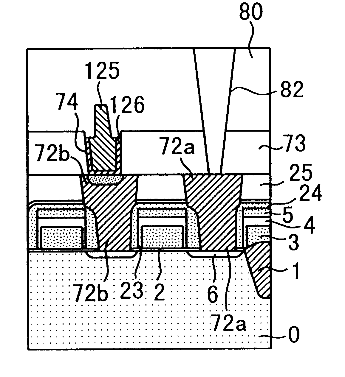
A first silicon oxide film is formed in such a manner as to cover source / drain regions of a transistor. A conductive pad is provided in the first silicon oxide film in such a manner that one end surface thereof is connected to each source / drain region and the other end surface thereof is exposed to the surface of the first silicon oxide film. A second silicon oxide film is formed on the first silicon oxide film and the pad. A conductive layer functioning as a plug is provided in the second silicon oxide film in such a manner that one end surface thereof is in contact with the pad and the other end surface thereof is connected to an interconnection layer. The surface of the first silicon oxide film is smoothly continuous to the other end surface of the pad at the same level. The conductive layer as the plug is formed in such a manner as to be smaller in size than the pad and to be in contact with the central portion of the pad.

Description

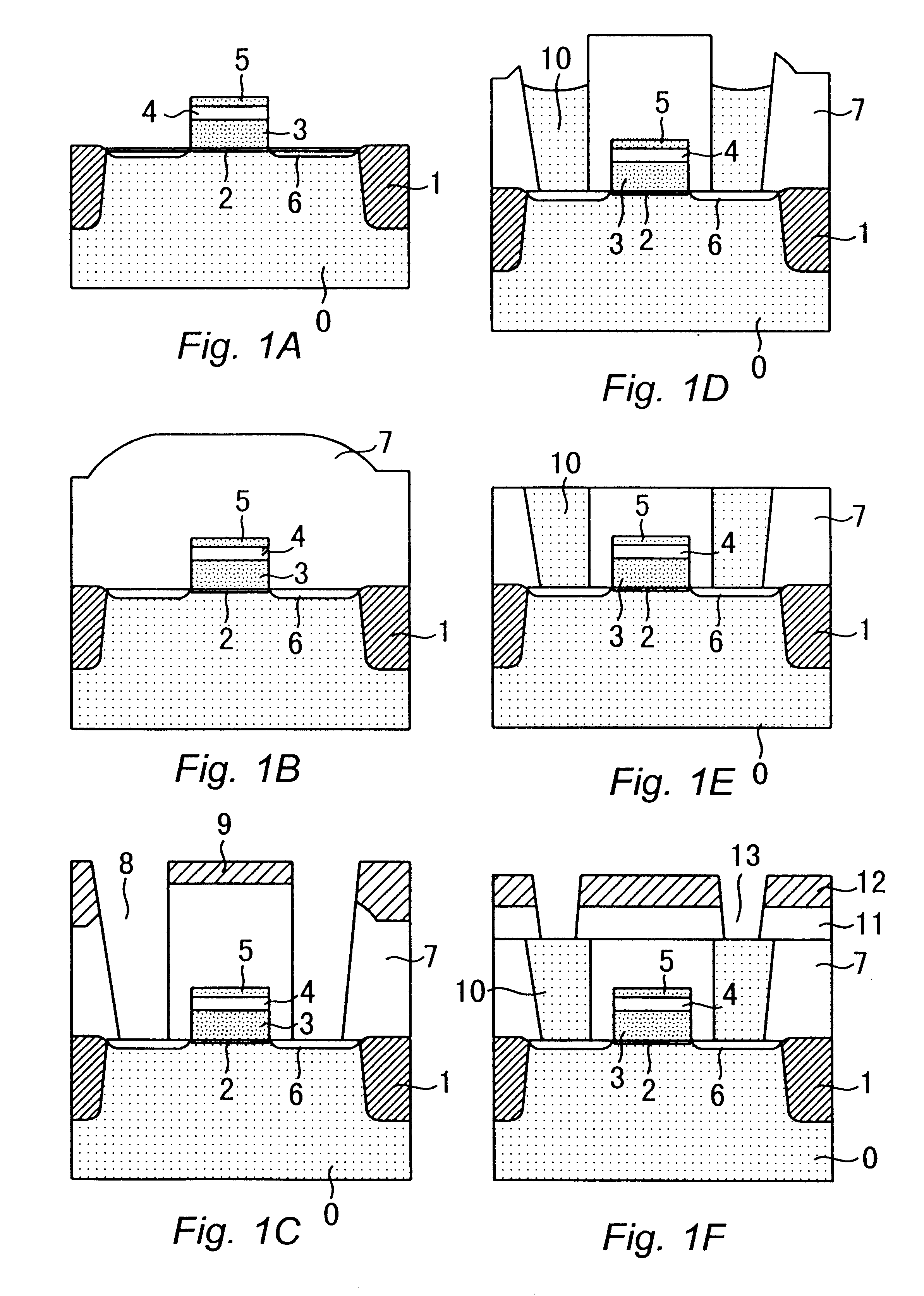
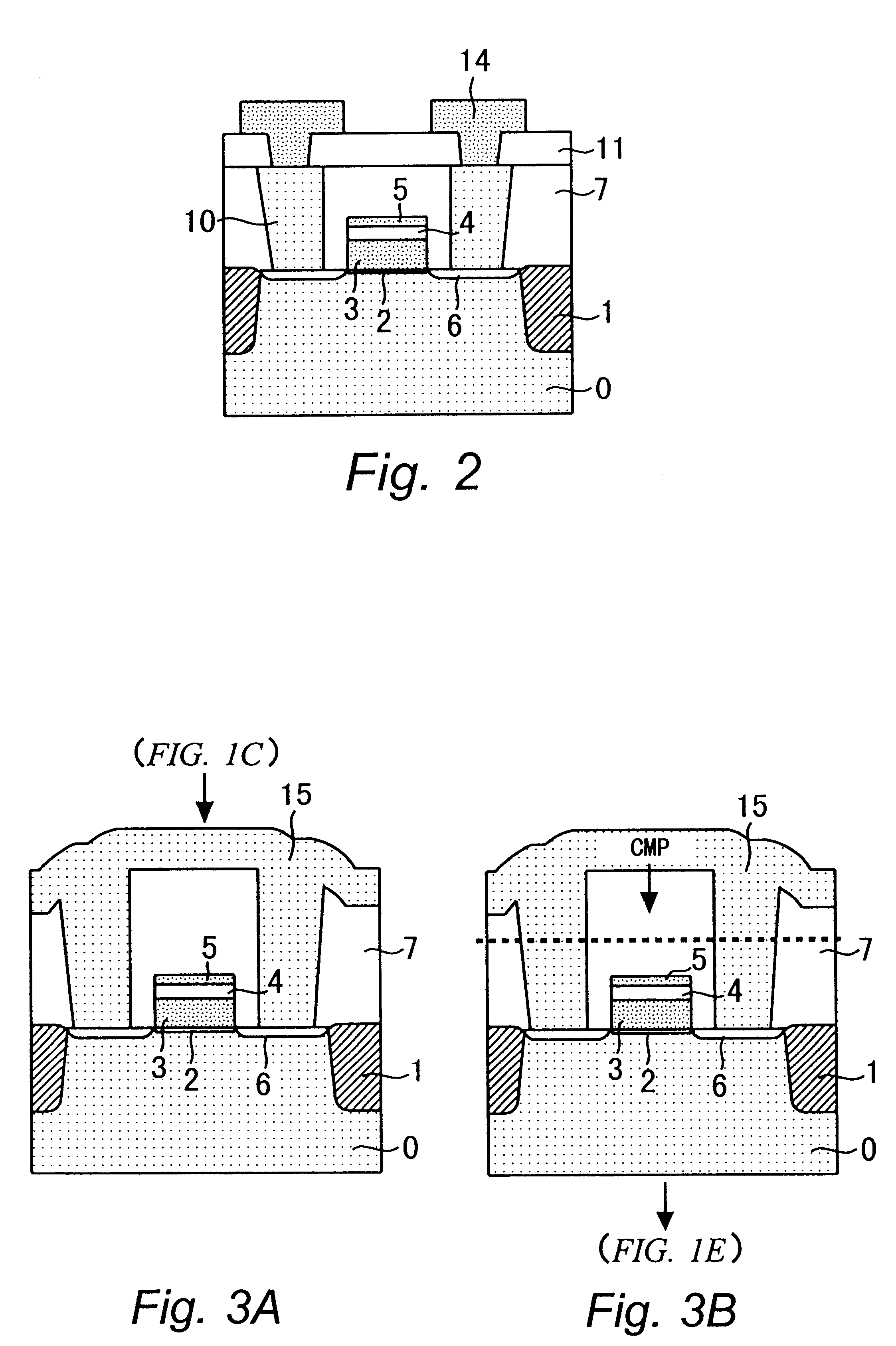
1. Field of the InventionThe present invention generally relates to a semiconductor device and a manufacturing method thereof, and particularly to a semiconductor device having a multi-layer interconnection structure and a manufacturing method thereof.2. Description of the Background ArtFIGS. 40A to 40F are views illustrating a related art structure of a semiconductor device having a multi-layer interconnection structure and a manufacturing method thereof. Referring to FIG. 40A, reference numeral 0 designates a silicon substrate; 1 is a trench isolation region; 2 is a gate oxide film; and 3 is a gate silicon film deposited by low pressure CVD (Chemical Vapor Deposition). The gate silicon film 3 is made from polysilicon or amorphous silicon doped with an impurity such as phosphorus (P) or arsenic (As).In FIG. 40A, reference numeral 4 is a silicon oxide film deposited by low pressure CVD, and 5 is a silicon nitride film deposited by low pressure CVD. The gate silicon film 3, the silic...

Claims


Application Information

Patent Timeline
IPC IPC(8): H01L21/70H01L21/60H01L23/52H01L23/522H01L21/02H01L21/768H01L21/8242H01L23/532H01L27/108H01L21/822H01L27/00H01L27/04
CPCH01L21/76802H01L21/76804H01L21/76805H01L21/76829H01L21/76834H01L21/76889H01L21/76895H01L21/76897H01L23/5226H01L27/10855H01L2924/0002H01L23/53223H01L23/53228H01L27/10814H01L27/10888H01L28/84H01L28/90H01L2924/00H01L21/76831H10B12/315H10B12/485H10B12/0335H01L21/768
Inventor TANAKA, YOSHINORI
Owner RENESAS ELECTRONICS CORP
Learn More