Content Addressable Memory array, cell, and method using 5-transistor compare circuit and avoiding crowbar current

a technology of content addressable memory and compare circuit, applied in the field of digital integrated circuit, can solve the problems of consuming considerable power, consuming more space on an integrated circuit than may be desirable, and consuming considerable power

Inactive Publication Date: 2002-05-07
TALITY
View PDF4 Cites 27 Cited by
  • Summary
  • Abstract
  • Description
  • Claims
  • Application Information

AI Technical Summary

Benefits of technology

A CAM core cell has been designed capable of storing two binary bits, comprising a data bit and a mask bit. This cell can take on a total of four possible states: logic one, logic zero, and two possible don't-care states: don't-care-one, and don't-care-zero. The cell contains comparison circuitry for detecting match condit

Problems solved by technology

Cells of these arrays produce a match compare result if the query input is equal to the data stored in the cell, and a mismatch result otherwise.
Cells of these "ternary CAM" arrays produce a match compare result if the query input is either equal to the data stored in the cell, or the cell contains a don't care state, and a mismatch resul

Method used


Image

  • Content Addressable Memory array, cell, and method using 5-transistor compare circuit and avoiding crowbar current
  • Content Addressable Memory array, cell, and method using 5-transistor compare circuit and avoiding crowbar current
  • Content Addressable Memory array, cell, and method using 5-transistor compare circuit and avoiding crowbar current

Examples


Embodiment Construction

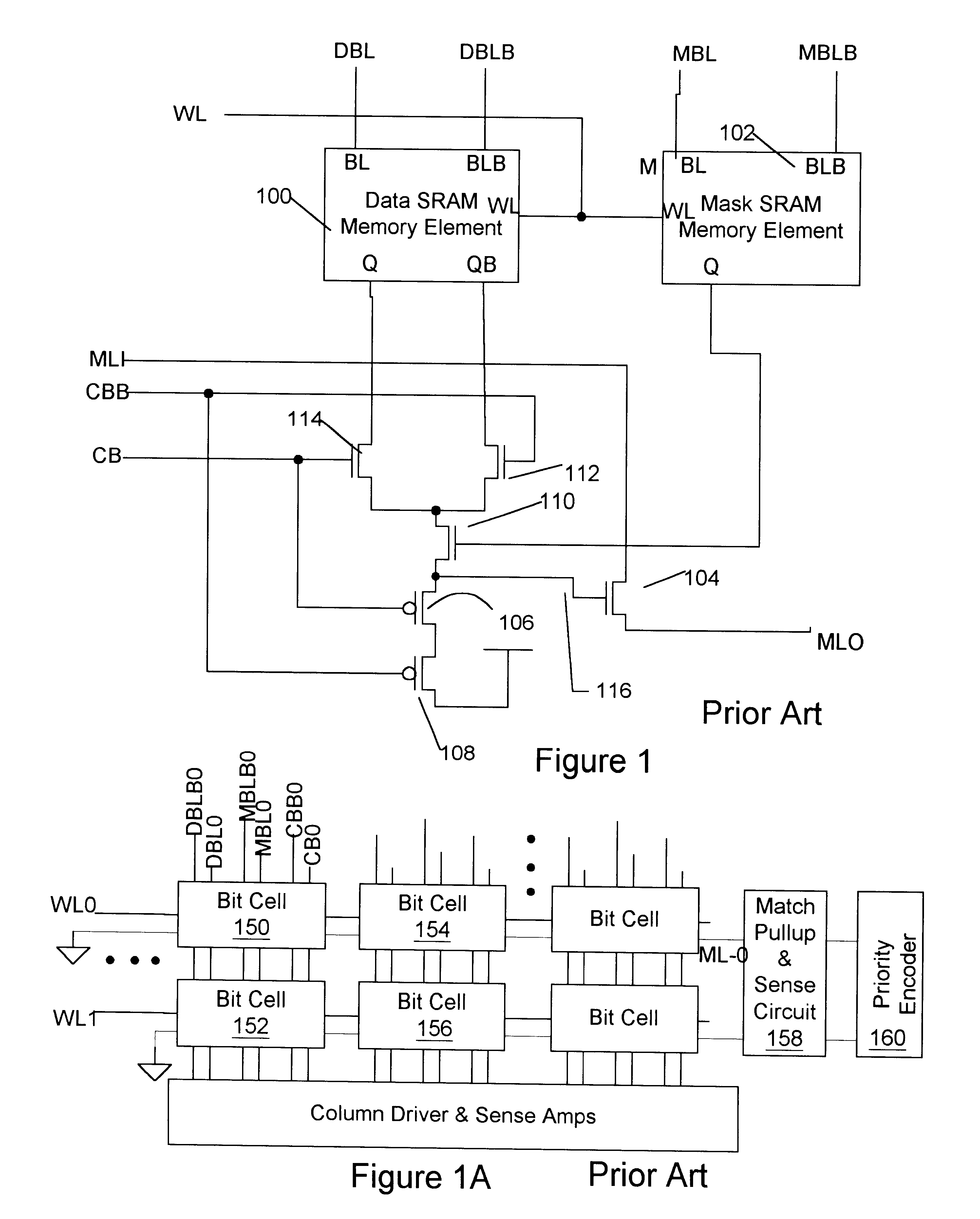
A ternary-CAM bit cell design as known in the art has a data static-random-access-memory (SRAM) element 100 (FIG. 1) and a mask SRAM element 102. SRAM elements 100 and 102 may be six transistor static RAM elements as known in the art and illustrated in FIG. 1B. Alternatively, SRAM elements 100 and 102 may be four-transistor-plus-two-resistor "poly load" static RAM elements as known in the art. A number of these bit cells are formed into an array, as depicted in FIG. 1A, having a plurality of rows and a plurality of columns. The data SRAM element 100 (FIG. 1) and mask SRAM element 102 have write enable inputs that are coupled to a write line WL common to several cells, such as WL0 common to cells 150 and 154, of a row. The data SRAM element 100 of each cell is coupled to data DBL and data complement DBLB input / output lines common to several cells of a column, such as DBL0 and DBLB0 common to cells 150 and 152. The mask SRAM element 102 is coupled to mask MBL and mask complement MBLB ...


PUM


Abstract

A content addressable memory system has rows and columns of CAM cells. Each CAM cell has a data memory, and comparison circuitry for comparing the data bit of the memory element with a compare data, and for driving a signal onto a match line when the data bit is not equal to the compare data. The comparison circuitry has a mismatch node with a pre-discharge device, and drives a match line drive device coupled to the match line. The mismatch node also couples to a first comparison device having source an output of the data memory and gate coupled to the compare data, and a second comparison device having source a second output of the data memory and gate coupled to compare data. Disclosed is a ternary implementation of the CAM cell also having a mask bit. Also disclosed is CAM timing such that the CAM cells operate without crowbar current.

Description

FIELD OF THE INVENTIONThe Invention relates to the field of digital integrated circuits, and in particular relates to the design of static CMOS Content-Addressable Memory (CAM) arrays. CAM arrays are a form of associative memory. In particular, the invention relates to cells and CAM arrays having bit cells capable of storing three or more content states including: "logic one", "logic zero", and at least one form of "don't care"; such CAM arrays are known as ternary CAMs.BACKGROUND OF THE INVENTIONCMOS CAM arrays are commonly used in cache systems, and other address translation systems, of high speed computing systems. They are also useful in high-speed network routers, and many other applications known in the art of computing.CAM arrays are characterized by circuitry capable of generating a "match" output indicating whether any location of the array contains a data pattern matching a query input, and the identity of that location. CAM arrays typically are comprised of multiple rows,...

Claims


Application Information

Patent Timeline
IPC IPC(8): G11C15/00G11C15/04
CPCG11C15/04
Inventor PETERSON, LUVERNE
Owner TALITY
Why Eureka
Try Eureka