Semiconductor memory module and module system

Inactive Publication Date: 2002-05-14
MITSUBISHI ELECTRIC CORP
View PDF5 Cites 60 Cited by
  • Summary
  • Abstract
  • Description
  • Claims
  • Application Information

AI Technical Summary

Problems solved by technology

However, the impedances are mismatched between the driver circuit and the transmission path due to a parasitic capacitance and a parasitic inductance which are incidental to a branch line connected to each module of the transmission path, and the signal is reflected and is thereby distorted in some cases.
When the signal is reflected, an overshoot or an undershoot is liable to be generated on the signal waveform.
When the ring

Method used


Image

  • Semiconductor memory module and module system
  • Semiconductor memory module and module system
  • Semiconductor memory module and module system

Examples


Embodiment Construction

>

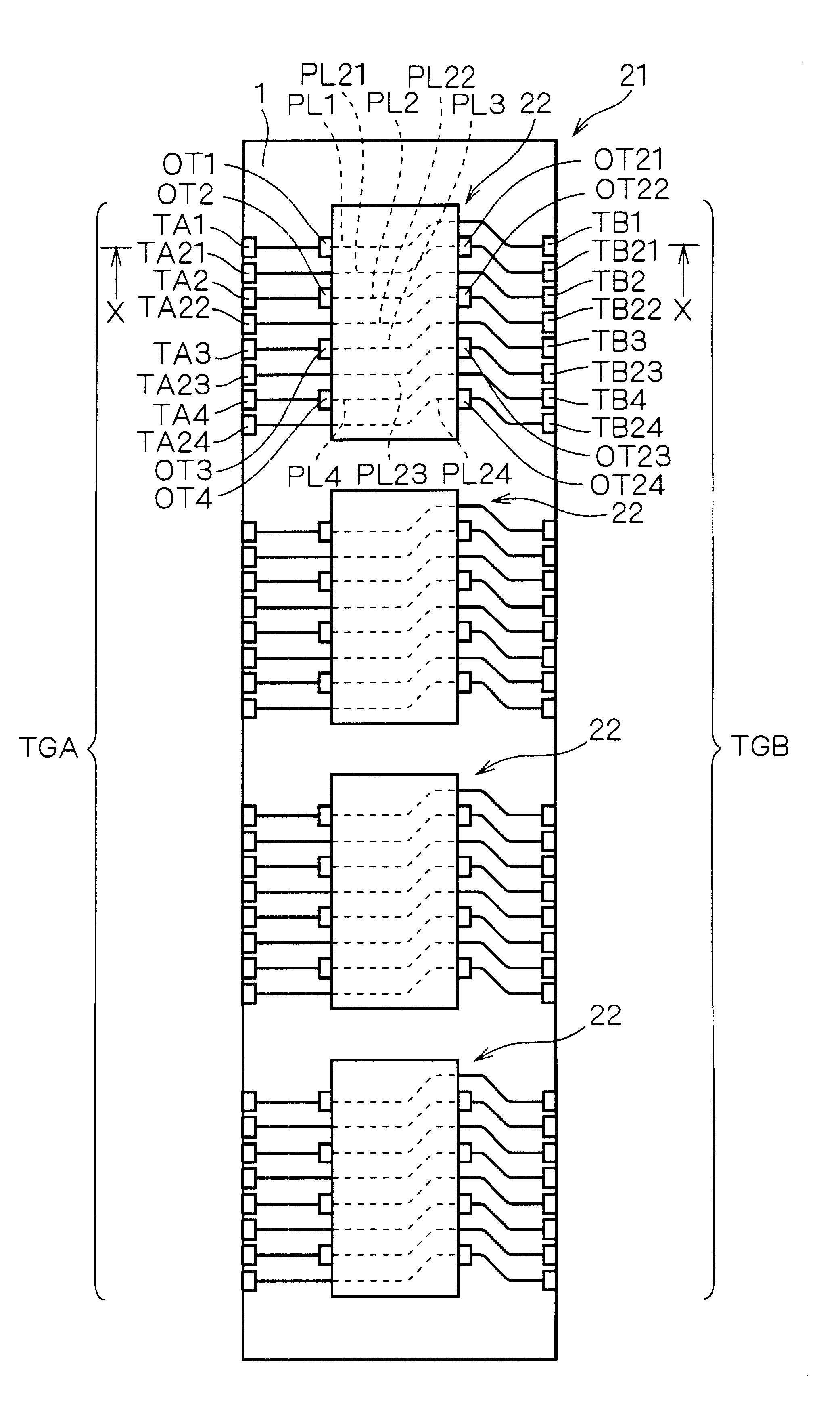
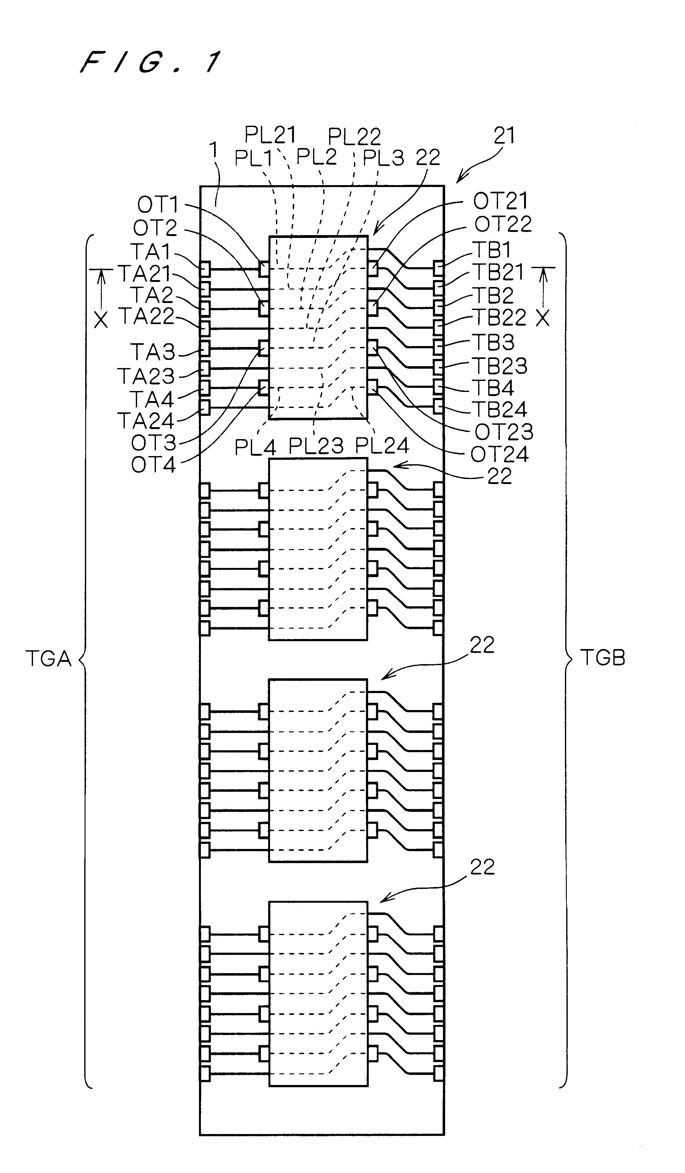
FIG. 1 is a plan view showing a basic structure of a semiconductor memory module according to the present invention, illustrating a memory module 21 having four DRAMs (Dynamic Random Access Memory) 22 mounted on a multilayer printed circuit board 1.

The multilayer printed circuit board 1 is provided with a plurality of boards (for example, six to eight layers) made of glass epoxy, and has an elongated rectangular shape such that the four ERAMs 22 are provided in a line corresponding to a direction of arrangement of external terminals thereof. Board terminal groups TGA and TGB of the module are provided to make a pair along two long sides of the multilayer printed circuit board 1.

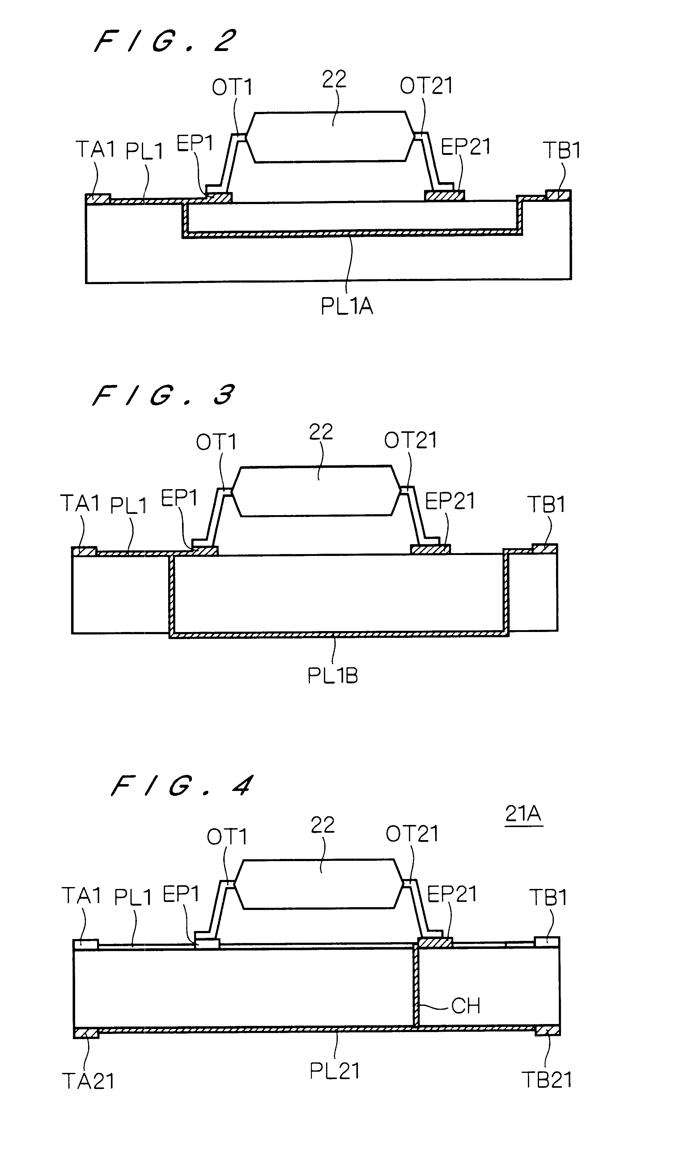
The DRAM 22 is a package referred to as a so-called type 2 of a TSOP (Thin Small Outline Package), and has an external terminal provided in two directions of the long side. The DRAM 22 typically represents an actual package and the number and shape of the external terminals are simplified.

Moreover, all the D...


PUM


Abstract

Provided is a semiconductor memory module capable of decreasing a parasitic capacitance and a parasitic inductance which are incidental to a signal transmission path, thereby reducing a distortion of a signal waveform. In a memory module, four DRAMs are provided on a muttilayer printed circuit board in one line corresponding to a direction of arrangement of external terminals thereof and board terminal groups of the module are provided to make a pair along two long sides of the multilayer printed circuit board. The DRAM has external terminals extended from one of the long sides and external terminals extended from the other long side. Board terminals and board terminals in the board terminal group of the module are connected to the DRAM, and board terminals and board terminals in the board terminal group TGB of the module are connected to the DRAM.

Description

1. Field of the InventionThe present invention relates to a semiconductor memory module and more particularly to a structure of a semiconductor memory module corresponding to a high speed operation.2. Description of the Background ArtWith an increase in a processing speed of a semiconductor device, a speed of a signal transmitted and received between semiconductor devices is also increased. In particular, a digital signal has short rise and fall times.When the rise and fall times of the signal are shortened, a signal is easily distorted over a printed circuit board on which the semiconductor device is to be mounted. Examples of the distortion include the case in which an overshoot voltage and an undershoot voltage are raised, the case in which a signal waveform becomes step-shaped when the waveform is, raised to reach a predetermined level, and the like.The case in which a plurality of semiconductor memory modules having a plurality of semiconductor memories provided thereon are mou...

Claims


Application Information

Patent Timeline
IPC IPC(8): G11C5/00H05K1/14H05K1/11
CPCG11C5/04G11C5/06H05K1/117H05K1/14H05K1/0295H05K1/114H05K2201/10159H05K1/142H05K2201/09954H05K2201/10189H05K2201/10689H05K2203/1572
Inventor TOBITA, YOUICHI
Owner MITSUBISHI ELECTRIC CORP
Why Eureka
Try Eureka