

Etch method using a dielectric etch chamber with expanded process window
- Summary
- Abstract
- Description
- Claims
- Application Information
AI Technical Summary
Benefits of technology
Problems solved by technology
Method used
Image

Examples
example 1
Table 1--Example 1
We expect that a pattern of square depressions or protrusions 60 as shown in FIG. 14 would be preferable to the pyramid-shaped depressions actually tested, because the square features have a greater surface area. As stated earlier, we expect that maximizing the surface area of the surface contour is advantageous in order to maximize the adhesion of the material deposited thereon.
We installed the roof in a conventional plasma etch chamber and performed the same plasma etch process performed in the Control. We found that the third quadrant of the roof exhibited the best polymer adhesion. Compared to the smooth first quadrant, we were able to process 2.5 times more wafers before material deposited on the third quadrant began flaking. At this point, the polymer layer deposited on the third quadrant had a thickness of 1.2 mm, which is 85% thicker than the maximum polymer thickness that could be deposited on a conventional smooth or bead blasted surface without flaking.
B...
example 2
Table 2--Example 2
Example 3
Hemispherical Depressions in Aluminum Oxide Roof
We fabricated a roof of a 0.5 inch (13 mm) thick plate of aluminum oxide (alumina) ceramic. Alumina has a much lower thermal conductivity than aluminum nitride, but it has the advantage of being readily machinable. We created the pattern of depressions shown in FIGS. 16 and 17 by drilling in the alumina an array of approximately hemispherical holes, or holes having an arcuate cross section, having a hole diameter W of 4 mm and a spacing S between the perimeters of adjacent holes of 1 mm. We tested two prototypes in which the depth of the holes (the topographical feature height H) were 1 mm and 2 mm, respectively. Both prototypes exhibited no flaking of the polymer deposits.
example 4
Square Protrusions in Anodized Aluminum
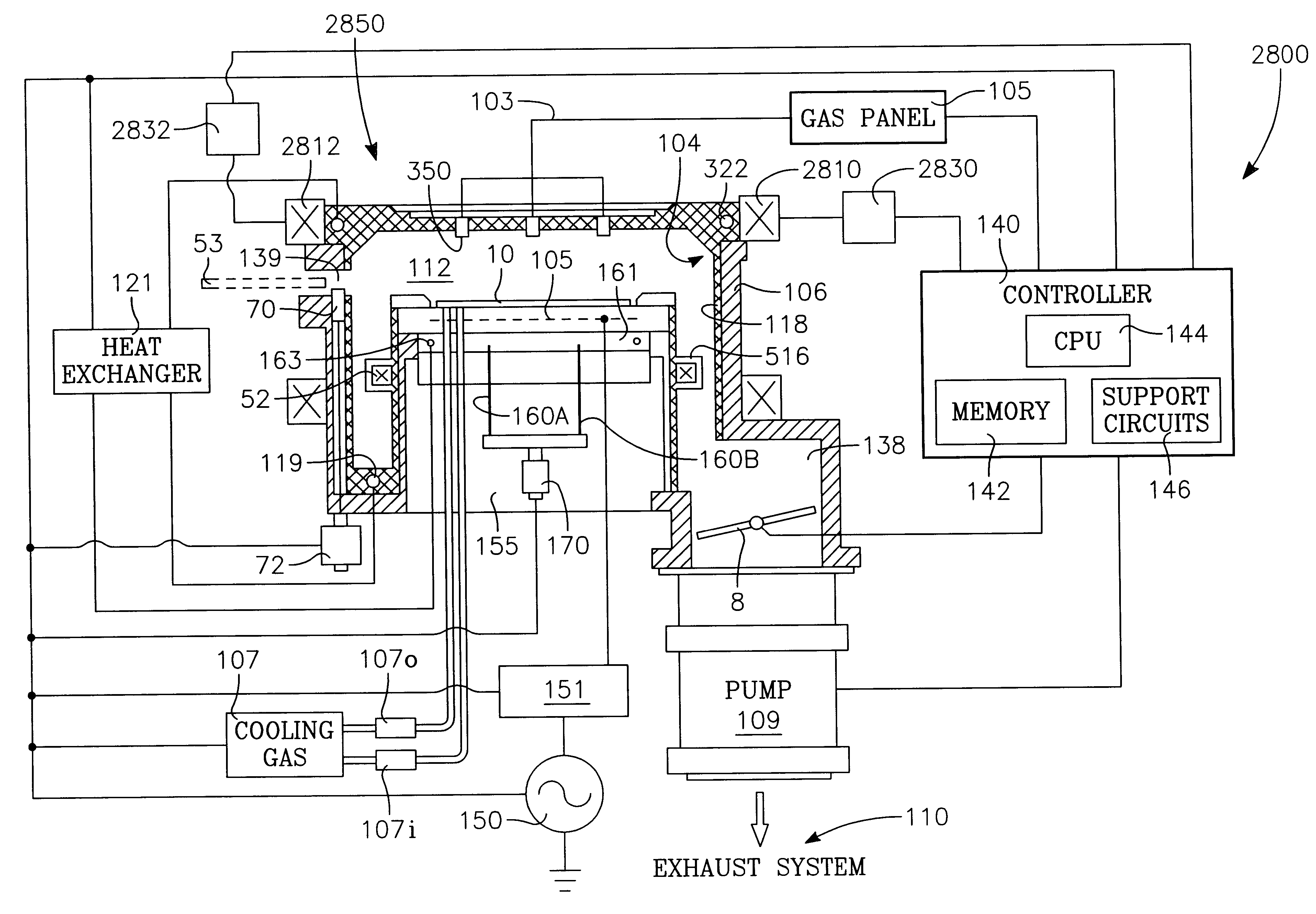
FIGS. 13 and 14 show an aluminum roof in which we machined an array of square protrusions. While the section is illustrated as solid the same features or protrusions may be incorporated into the top ceiling 316 having a plurality of gas inlets 350 or mini-gas distribution plates 220. The aluminum was anodized after the machining. In one prototype the protrusions had 1 mm width W, 1.5 mm height H, and 3 mm spacing S. In a second prototype, the protrusions had 2 mm width W, 2 mm height H, and 5 mm spacing S. Both prototypes exhibited no flaking of the polymer deposits.
In the second prototype, we also tested an implementation of the gas inlet holes in the gas distribution plate. Instead of a conventional array of gas inlet holes uniformly distributed over the surface of the plate, we installed in the plate only eleven quartz discs (not shown), where each quartz disc was 10 mm diameter and included eleven gas inlet holes 0.6 mm diameter.
PUM
 Abstract
Description
Claims
Application Information