Re-oxidation approach to improve peripheral gate oxide integrity in a tunnel nitride oxidation process

a tunnel nitride and oxidation process technology, applied in the field of memory devices, can solve the problems of oxide damage, difficult fabrication of tunnel oxides in memory cells, and difficult reliability of tunnel oxides

Inactive Publication Date: 2002-08-20
MONTEREY RES LLC
View PDF9 Cites 13 Cited by
  • Summary
  • Abstract
  • Description
  • Claims
  • Application Information

AI Technical Summary

Benefits of technology

The present invention is for a process for fabricating a semiconductor device, and more preferably, a memory device. Although the following description is described with respect to fabricating an EEPROM device, it will be recognized by those skilled in the art that the following description can not only be applied to fabricating any non-volatile memory device, such as a one-bit or two-bit EEPROM device, but to any semiconductor device as well, such as a capacitor, a diode, a resistor, an amplifier, a memory chip, a microchip, an integrated circuit, a transistor, a digital signal processor, and a logic chip.

Problems solved by technology

While the recent advances in EEPROM technology have enabled memory designers to double the memory capacity of EEPROM arrays using two-bit data storage, numerous challenges exist in the fabrication of material layers within these devices.
In particular, fabricating a tunnel oxide within a memory cell presents several challenges.
For example, the reliability of the tunnel oxide can be problematic.
The problems with the reliability of the tunnel oxide are often associated with charge trapping and oxide damage during the programming and erasing cycles within the memory cell.
The damaged tunnel oxide may cause memory data retention problems and may also result in the failure of the memory cell.
There are several problems that occur with the above-described method for fabricating a memory cell.
One problem is that during the oxynitridation process, nitrogen, which is introduced into the tunnel oxide, can also enter into and contaminate the gate oxide in the peripheral gate region.
Nitrogen introduced into the semiconductor substrate will often form a bond with the silicon atoms in the semiconductor substrate, and thus, make it very difficult to remove the nitrogen from the semiconductor substrate.
For example, the nitrogen that is contaminating the semiconductor substrate cannot be effectively removed by using a conventional hydrofluoric acid etch process.
Additionally, the presence of the contaminate nitrogen contributes to non-uniform oxide growth during a subsequent growth of a gate oxide layer.
Since the oxynitridation process degrades the characteristics of the gate oxide layer in a peripheral gate region of the memory cell, the oxynitridation approach is less attractive for manufacturing memory cells.

Method used


Image

  • Re-oxidation approach to improve peripheral gate oxide integrity in a tunnel nitride oxidation process
  • Re-oxidation approach to improve peripheral gate oxide integrity in a tunnel nitride oxidation process
  • Re-oxidation approach to improve peripheral gate oxide integrity in a tunnel nitride oxidation process

Examples


Embodiment Construction

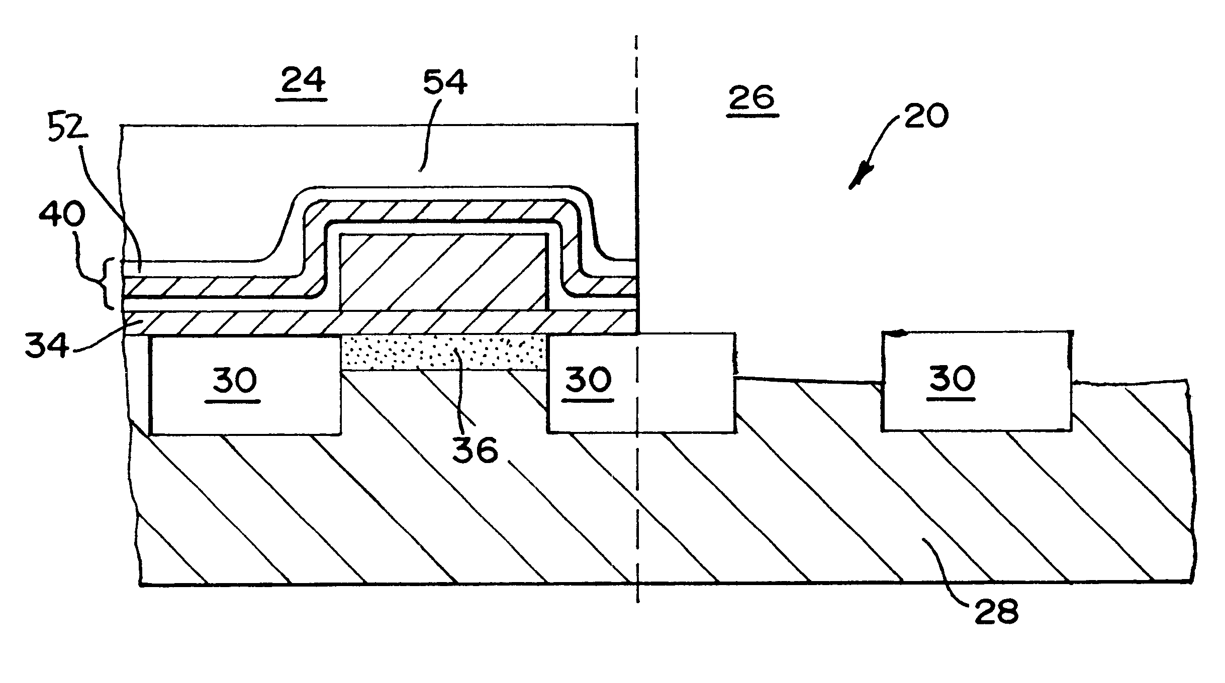
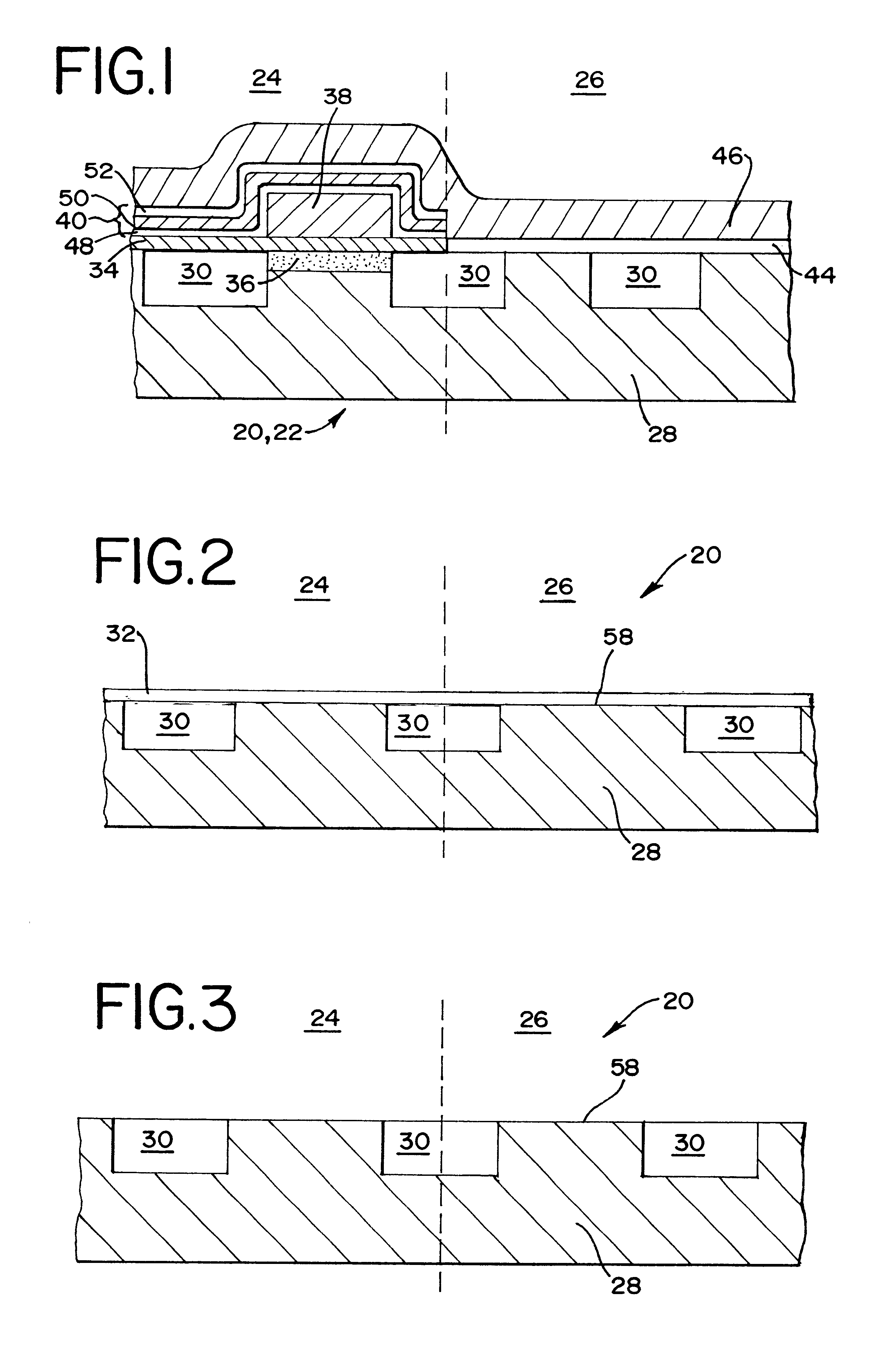
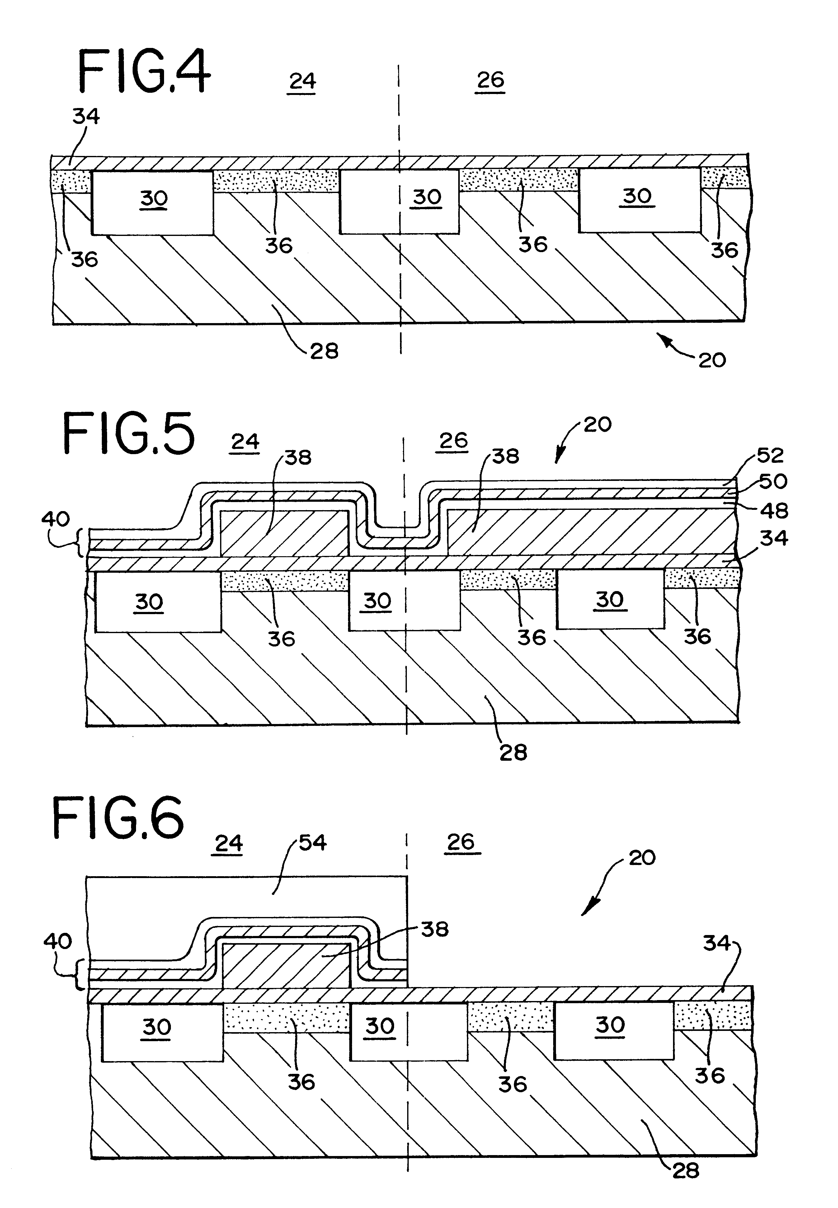
Shown in FIG. 1, in cross-section, is a semiconductor device 20, and in particular, a memory device 22. The semiconductor device 20 includes any semiconductor device known to those skilled in the art, such as a capacitor, a diode, a resistor, an amplifier, a memory chip, a microchip, an integrated circuit, a transistor, a digital signal processor, and a logic chip. Memory device 22 includes any memory device known by those skilled in the art, such as a RAM device, a DRAM device, an SDRAM device, a ROM device, an NROM device, and PROM device, an EEPROM device such as a one-bit or two-bit EEPROM device, and any non-volatile memory device known to those skilled in the art. Please note that FIGS. 1-9 illustrate only a portion of the memory device 22 and that memory device 22 may include many memory cells within memory device 22. For the sake of clarity, these additional memory cells have been left out of FIGS. 1-9.

Memory device 22 includes a semiconductor substrate 28 having a core regi...


PUM


Abstract

A process for fabricating a semiconductor device 20 that includes providing semiconductor substrate 28 having a core region 24 and a peripheral gate region 26. The semiconductor substrate 28 has at least one shallow trench isolation region 30 and at least one nitrogen-contaminated region 36 in the peripheral gate region 26. A tunnel oxide layer 34 overlies the semiconductor substrate 28 and a first polysilicon layer 38 overlies the tunnel oxide layer 34 in the core region 24. An ONO layer 40 overlies the first polysilicon layer 38 in the core region 24. The process further includes growing a sacrificial oxide layer 42 overlying the nitrogen-contaminated region 36 in the peripheral gate region 26, wherein oxygen from within the sacrificial oxide layer 42 diffuses into the nitrogen-contaminated region 36 and forms silicon dioxide. By allowing oxygen from within the sacrificial oxide layer 42 to diffuse into the nitrogen-contaminated region 36 and form silicon dioxide, the nitrogen 56 can be removed from within the semiconductor substrate 28 by removing the silicon dioxide.

Description

This invention relates generally to semiconductor device. In particular, the present invention relates to a method and process for manufacturing a non-volatile memory device.Non-volatile memory devices are currently in widespread use in electronic components that require the retention of information when electrical power is terminated. Non-volatile memory devices include read-only-memory (ROM), programmable-read-only memory (PROM), erasable-programmable-read-only memory (EPROM), and electrically-erasable-programmable-read-only-memory (EEPROM) devices. EEPROM devices differ from other non-volatile memory devices in that they can be electrically programmed and erased. Flash EEPROM devices are similar to EEPROM devices in that memory cells can be programmed and erased electrically. However, Flash EEPROM devices enable the erasing of large blocks of memory cells in the device using a single electrical current pulse.Typically, an EEPROM device includes a floating-gate electrode within wh...

Claims


Application Information

Patent Timeline
Patent Type & Authority Patents(United States)
IPC IPC(8): H01L21/8247H01L21/8234H01L21/70H01L27/105H01L21/8239
CPCH01L21/823462H01L27/105H01L27/11526H01L27/11536H01L27/1052H10B99/00H10B41/40H10B41/44
Inventor FANG, HAOHE, YUE-SONG
Owner MONTEREY RES LLC
Why Eureka
Try Eureka