Methods for manufacture of self-aligned integrally gated nanofilament field emitter cell and array

a nanofilament field and nanofilament technology, applied in the field of field emitter cells and arrays, can solve the problems of high equipment and manufacturing costs, high spatial registration requirements for high resolution lithography, and difficult fabrication of vacuum electron sources for practical applications

Inactive Publication Date: 2002-08-27
SEC OF THE NAVY AS REPRESENTED BY THE UNITED STATES OF AMERICA THE
View PDF12 Cites 110 Cited by
  • Summary
  • Abstract
  • Description
  • Claims
  • Application Information

AI Technical Summary

Problems solved by technology

Effective methods generally require the use of lithography which has a number of inherent disadvantages including a high equipment and manufacturing cost.
For example, the high degree of spatial registration requires expensive high resolution lithography.
However, these vacuum electron sources are difficult to fabricate for practical applications.
In addition, thermionic sources must be heated, and thus require special heating circuits and power supplies.
Photoemitters have similar problems with regard to low currents and current densities.
On the other hand, high emission current from carbon nanotubes oriented parallel to the substrate has also been observed, which can be attributed to defects on the tube sidewalls.
However, these nanofilament electrodes are not gated and thus, have limited practical use as field emitters.
This and other presently available manufacturing techniques (all non-integral) fail to provide practical (e.g., in terms...

Method used


Image

  • Methods for manufacture of self-aligned integrally gated nanofilament field emitter cell and array
  • Methods for manufacture of self-aligned integrally gated nanofilament field emitter cell and array
  • Methods for manufacture of self-aligned integrally gated nanofilament field emitter cell and array

Examples


first embodiment

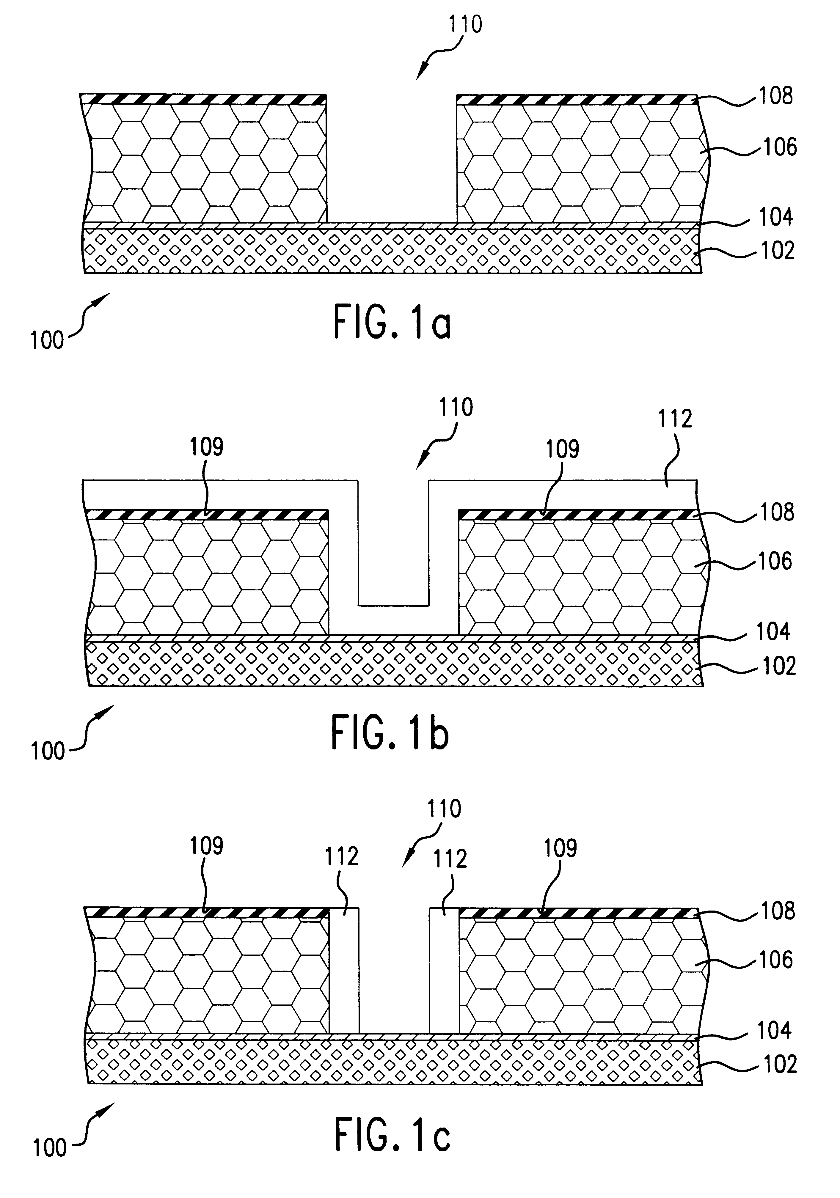
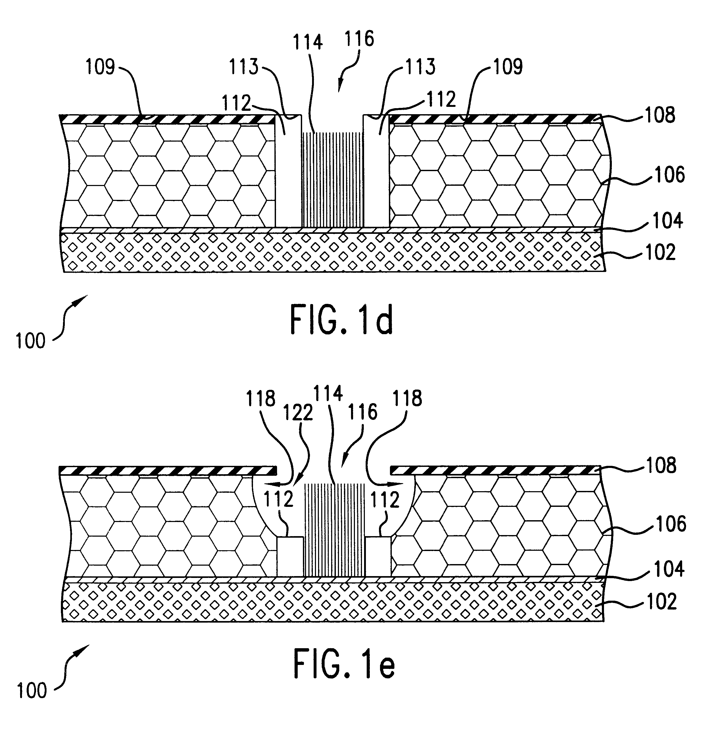
Referring now to FIGS. 1(a)-1(g), illustratively depicted therein are the steps of fabricating a field emitter cell 100 according to the present invention. The field emitter cell 100 is formed on a conductive or semiconductive substrate layer 102. Optimally, substrate layer 102 is a porous silicon substrate with a nanoporous layer in order to provide for highly directional nanotube growth.

A catalyst layer 104 is deposited on substrate layer 102 by sputtering or evaporative deposition of a suitable catalyst material. The catalyst layer promotes the growth of nanofilaments of interest under appropriate growth conditions (described below). For carbon nanotube growth, the most effective catalyst layer may comprise iron, nickel or cobalt.

Optionally, at this point, the catalyst-coated substrate may be annealed in air to anneal and oxidize the catalyst layer 104. Alternatively, the annealing / oxidation of catalyst layer 104 may be done later or it may be left unoxidized. Insulator layer 106...

2nd embodiment

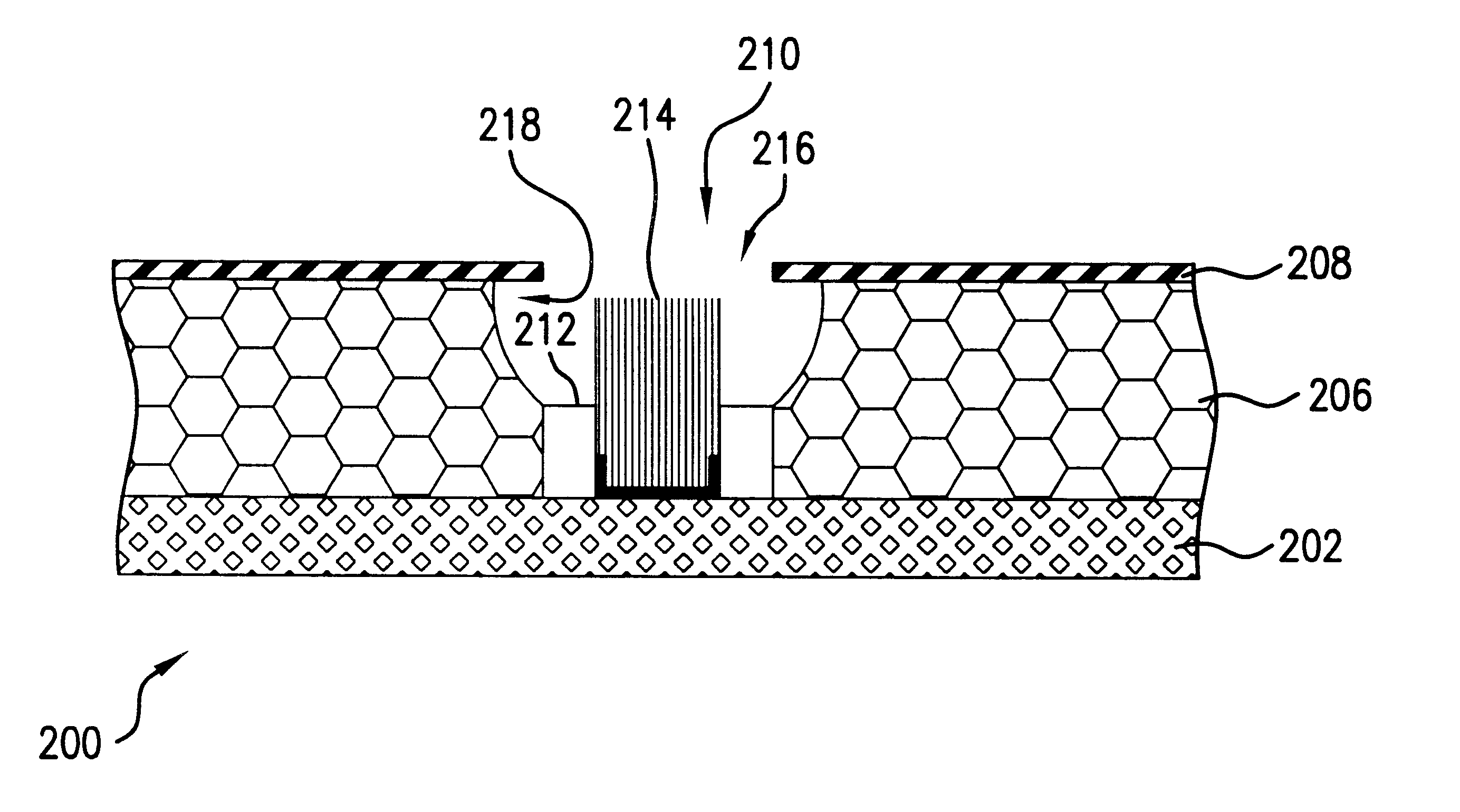
FIG. 2(a)-2(g) illustratively depict a second embodiment which differs from the first embodiment in that in the second embodiment, catalyst layer 204 is deposited after gate layer 208 and stand-off layer 212 are deposited and etched. Therefore, the various processing steps of the second embodiment are the same as in the first embodiment unless otherwise noted.

Insulator layer 206 is deposited directly on substrate layer 202 by any suitable manner known in the art. Subsequently, gate layer 208 is formed on insulator layer 206, and gate aperture 210 is patterned and etched. Stand-off layer 212 is deposited along the surface of cell structure 200 which includes along the gate layer horizontal surface 209, the vertical wall surfaces within gate aperture 210 and along surface 203 of substrate 202 exposed during the etching of gate aperture 210 (FIG. 2(b)). Next, stand-off layer 212 is removed from the horizontal surfaces of cell structure 200, namely gate layer horizontal surface 209 and ...

3rd embodiment

Referring now to FIGS. 3(a)-3(g), in a third embodiment, the starting substrate upon which the nanofilaments are grown is a post structure 330. Referring now specifically to FIG. 3(a), post 330 is formed by patterning and reactive ion etching (RIE) a starting material of nanoporous silicon layer substrate 302 with catalyst layer 304. The patterning and RIE are standard microelectronic fabrication methods known in the art. Catalyst layer 304 is optionally oxidized in the same manner as in the earlier described embodiments.

Nanofilaments 314 are preferably carbon nanotubes that are grown on top of post 330 under the same conditions as in the previous embodiments, resulting in clump cathode 316 (FIG. 3(b)). A conformal stand-off layer 312 composed of silicon nitride, silicon dioxide or tungsten, is deposited over the entire cell structure 300 structure (FIG. 3(c)).

Referring now to FIG. 3(d), planarization layer 332 is deposited over cell structure 300 along the top of stand-off layer 31...


PUM


Abstract

The present invention discloses a new field emitter cell and array consisting of groups of nanofilaments forming emitter cathodes. Control gates are microprocessed to be integrally formed with groups of nanofilament emitter cathodes on a substrate. Groups of nanofilaments are grown directly on the substrate material. As a result, the control gates and groups of nanofilaments are self-aligned with one another.

Description

1. Field of the InventionThe present invention relates to methods for manufacture of several distinct embodiments of a field emitter cell and array, in particular, to an integrally gated, self-aligned field emitter cell and array whose cathode is formed of a recently discovered class of materials of nanotubes and nanowires, collectively referred to as nanofilaments.2. Background of the InventionField emitters arrays (FEAs) are naturally small structures which provide reasonably high current densities at low voltages. Typically, FEAs are composed of emitter cells in the form of conical, pyramidal, or cusp-shaped point, edge or wedge-shaped vertical structures. Each cell is electrically insulated from a positively charged extraction gate and produces an electron beam that travels through an associated opening in the positively charged gate.The typical field emitter structure includes a sharp point at the tip of the vertical structure (field emitter) and opposite an electrode. In order...

Claims


Application Information

Patent Timeline
IPC IPC(8): H01L21/00H01J1/304H01J3/02
CPCB82Y10/00H01J1/304H01J3/021H01J2201/30469
Inventor HSU, DAVID S. Y.
Owner SEC OF THE NAVY AS REPRESENTED BY THE UNITED STATES OF AMERICA THE
Why Eureka
Try Eureka