

Multicolor organic EL element having plurality of organic dyes, method of manufacturing the same, and display using the same
a technology of organic el elements and organic dyes, which is applied in the direction of discharge tubes/lamp details, discharge tubes luminescnet screens, electric discharge lamps, etc., can solve the problems of inefficiency of color filter or blue color conversion methods, large amount of time and labor, and inability to manufacture high-definition displays. achieve the effect of high luminous efficiency and easy to provide multiple colors
- Summary
- Abstract
- Description
- Claims
- Application Information
AI Technical Summary
Benefits of technology
Problems solved by technology
Method used
Image

Examples
embodiment 1
(1) No Irradiation
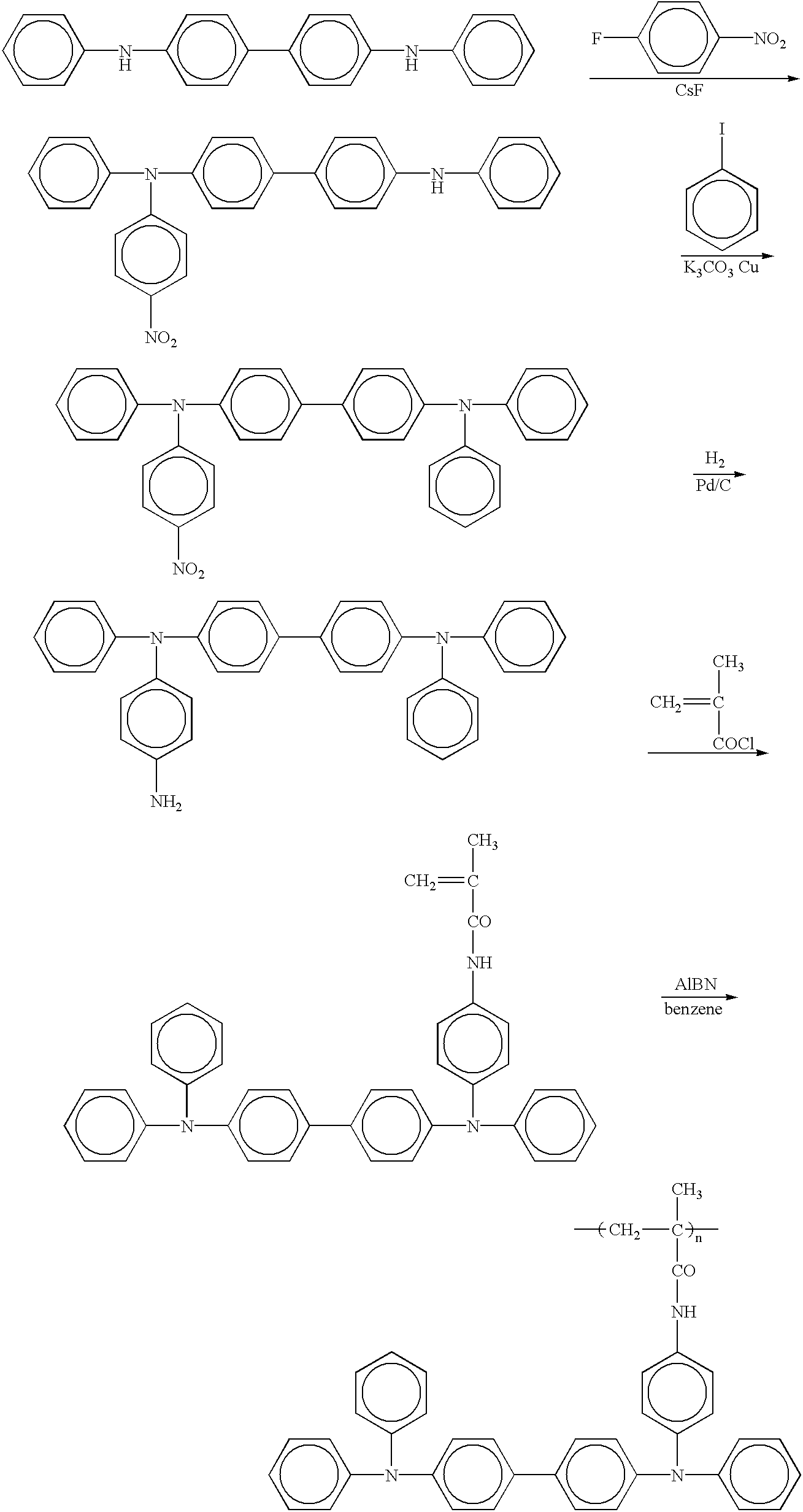
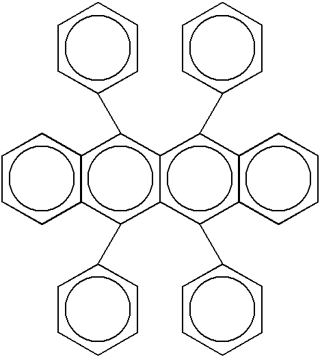
FIG. 1 is a sectional view illustrating a manufacturing process according to one embodiment of this invention. Reference number 1 designates a glass substrate on which ITO (indium-tin oxide) 2 of sheet resistance 15 .OMEGA. / .quadrature. is coated. A solution in 1,2-dichloroethane of polymer PTPDMA synthesized as described above, which has positive transporting capability, emits a blue-purple light, containing 1 wt. %, 3 wt. %, 5 wt. %, or 7 wt. % of rubrene based on the PTPDMA, which emits a yellow light and has the following formula: ##STR2##
was used to form a polymer layer 3 (rubrene-dispersed PTPDMA layer) of 600 .ANG. thickness on the ITO by means of spin-coating.
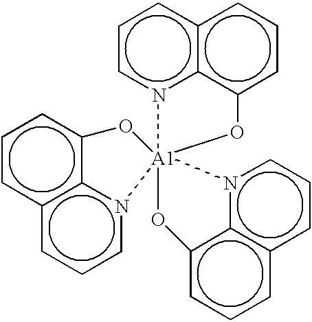
A tris(8-quinolinolate)aluminum complex layer (hereafter referred to as Alq) 4 with green emission and expressed by the following formula: ##STR3##
was formed on said polymer layer 3 as an electron transport layer 4 by depositing the material up to 400 .ANG. in a vacuum of 10.sup.-5 Torr. Finally, in th...
embodiment 2
(1) No Irradiation
FIG. 5 is a sectional view of Embodiment 2. Reference number 1 designates a glass substrate on which ITO (indium-tin oxide) 2 of sheet resistance 15 .OMEGA. / .quadrature. is coated. A positive hole-transport layer 6 was formed on the ITO by depositing N,N'-bis(3-methylphenyl)-1,1'-biphenyl-4,4'-diamine (hereafter referred to as TPD) which has a positive hole transporting capability and has the following formula ##STR4##
up to 400 .ANG. thickness In a vacuum of 10.sup.-6 Torr. Next, an Alq-rubrene layer 7 was formed as an electron transporting light emitting layer 7 by depositing Alq and rubrene thereon up to 600 .ANG. in a vacuum of 10.sup.-5 Torr., so that the ratio of Alq to rubrene was 97 wt. % and 3 wt. %. Finally, Mg and Ag (10:1) were co-deposited up to 2000 .ANG. under the same vacuum, as a rear electrode 5, acting as a negative electrode. The light-emitting area was 0.5 cm.times.0.5 cm.
In this organic EL element, a direct current voltage was applied to produc...
embodiment 3
(1) No Irradiation
FIG. 6 is a sectional view of Embodiment 3. Reference number 1 designates a glass substrate on which ITO (indium-tin oxide) 2 of sheet resistance 15 .OMEGA. / .quadrature. is coated. A 1,2-dichloroethane solution containing 30 wt. % of electron-transporting 1,3,4-oxadiazole (PBD), 5 wt. % of 1,1,4,4-tetraphenyl-1,3-butadiene (hereafter referred to as TPB) that is a blue-light-emitting dye, and 3 wt. % of rubrene, in a poly(N-vinylcarbazole) (PVK) capable of transporting positive holes and having an emission peak in the blue-purple wavelength region (410 to 420 nm) was used to form a polymer film 8 of 1000 .ANG. on the ITP by means of spin-coating. Finally, a layer 5 of Mg and Ag (10:1) was co-deposited up to 2000 .ANG. under the same vacuum as a negative electrode. The light-emitting area was 0.5 cm.times.0.5 cm.
In this organic EL element, a direct current voltage was applied to produce emission from the light emitting layer, using ITO and Mg:Ag, respectively, as pos...
PUM
| Property | Measurement | Unit |
|---|---|---|
| Color | aaaaa | aaaaa |
Abstract
Description
Claims
Application Information