Method for producing GaN-based compound semiconductor and GaN-based compound semiconductor device

Inactive Publication Date: 2002-11-05
NITRIDE SEMICON
View PDF28 Cites 58 Cited by
  • Summary
  • Abstract
  • Description
  • Claims
  • Application Information

AI Technical Summary

Problems solved by technology

However, in this ELO method, a reduction in dislocation density occurs only at the portions of the GaN layer where the SiO.sub.2 mask exists, and only these portions exhibit good properties.
However, even in this method, high dislocation density occurs in the low-temperature buffer layer, so that high dislocation density also occurs in the GaN or GaAlN layer formed thereon.
This is not satisfactory in obtaining a luminous device that i

Method used


Image

  • Method for producing GaN-based compound semiconductor and GaN-based compound semiconductor device
  • Method for producing GaN-based compound semiconductor and GaN-based compound semiconductor device
  • Method for producing GaN-based compound semiconductor and GaN-based compound semiconductor device

Examples


Example

Preferred embodiment of the present invention will hereinafter be described with reference to the drawings.

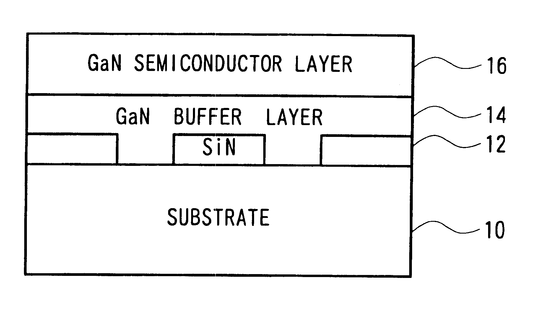
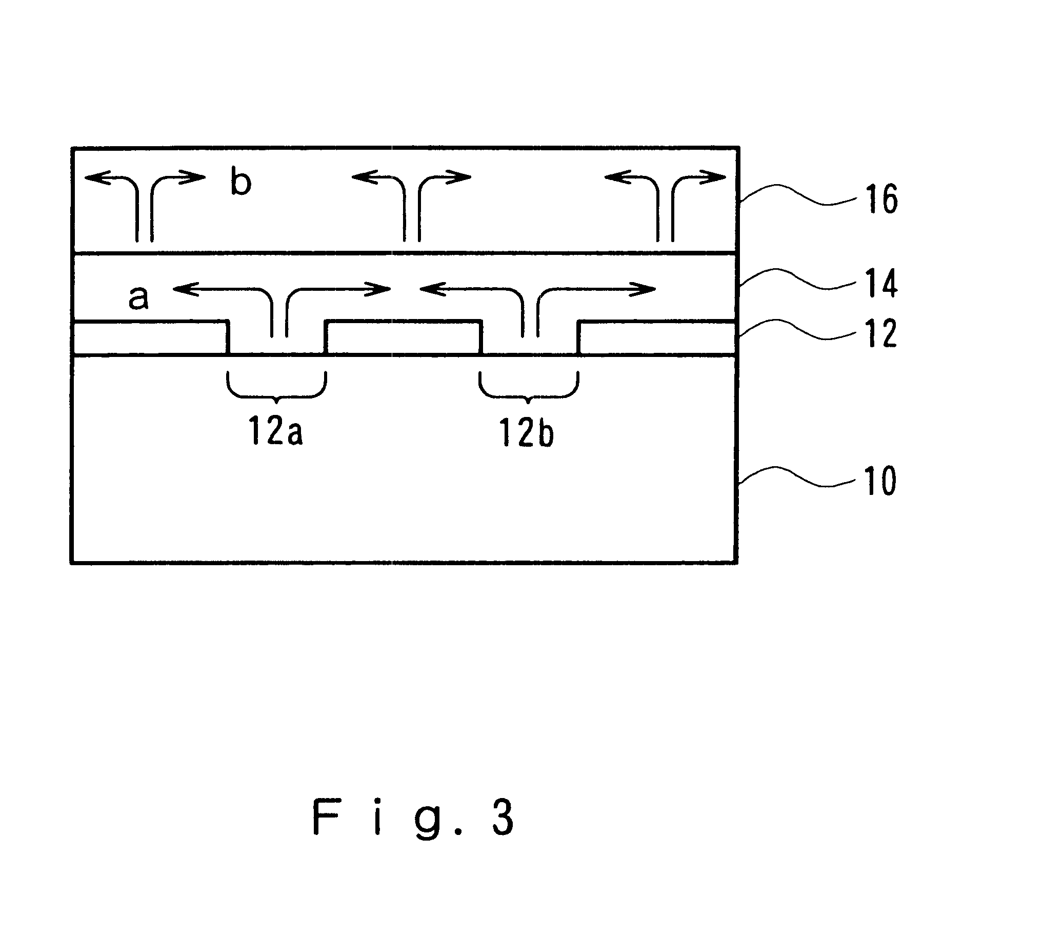
FIG. 1 shows the structure of a GaN-based compound semiconductor produced by the method of a first preferred embodiment. A SiN buffer body 12 is formed discretely on a substrate 10 such as sapphire. On the SiN 12, a GaN buffer layer 14 having a thickness of about 20 nm is formed at low temperatures (such as 500.degree. C.) and then a GaN semiconductor layer 16 having a thickness of about 2 .mu.m is formed thereon at high temperatures (such as 1,075.degree. C.).

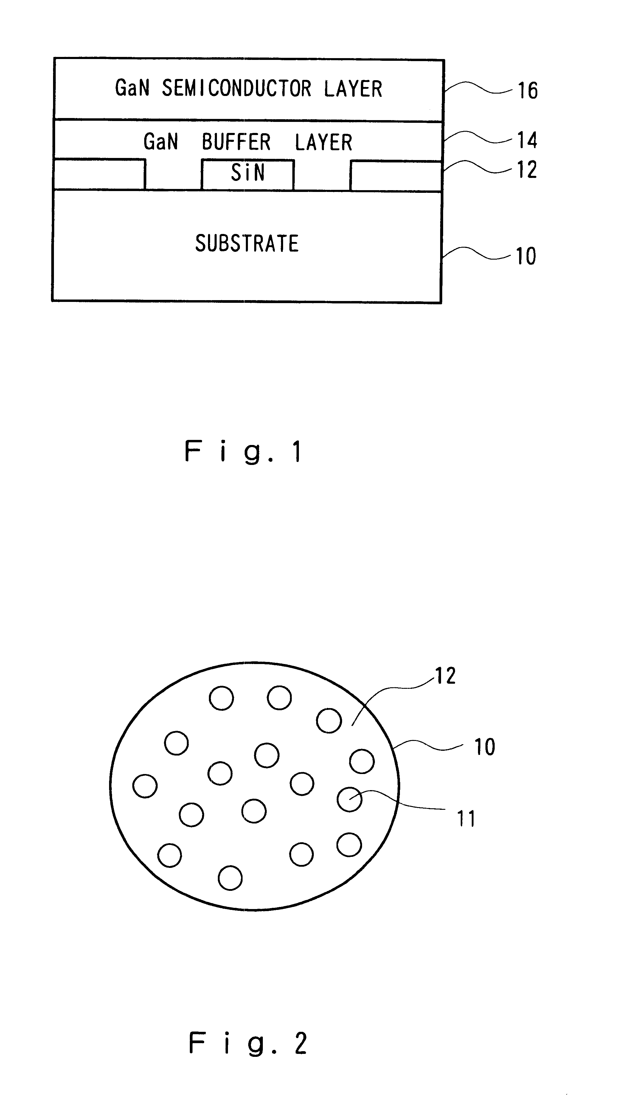
FIG. 2 is a schematic plan view of the SiN buffer body 12 formed on the substrate 10. The SiN buffer body 12 is formed, not in the form of a layer to cover the substrate 10. but discretely. so as to have pores 11, as shown in FIG. 2. That is, a plurality of buffer bodies are discretely formed or a buffer body having a plurality of pores is formed. The SiN buffer body 12 is not formed on the pores 11; that is, the substrat...


PUM


Abstract

A production method of a GaN-based compound semiconductor having excellent crystallinity and a GaN-based semiconductor device produced therefrom. A discrete SiN buffer body is formed on a substrate, and a GaN buffer layer is formed thereon at low temperatures and a GaN semiconductor layer is then formed at high temperatures. By forming the discrete SiN buffer body, the crystal growth, which is dependent on the substrate, of the low-temperature buffer layer is inhibited and monocrystallization is promoted to generate seed crystals used at the time of growing the GaN buffer layer. Further, by forming SiO2 discretely between the substrate and the SiN buffer body or by forming InGaN or a superlattice layer on the GaN semiconductor layer, distortion of the GaN semiconductor layer is reduced.

Description

(i) Field of the InventionThe present invention relates to a method for producing a gallium nitride-based compound semiconductor on a substrate.(ii) Description of the Related ArtGallium nitride-based semiconductors are widely used in luminous devices such as LEDs, and in other applications. In production of GaN semiconductors, a blue laser which is operable continuously over 10,000 hours at room temperature has been reported (S. Nakamura et al, Apply.Phys.Lett.72, 211(1998)) for growing GaN on a sapphire substrate by using an ELO (Epitaxially Laterally Overgrown) method. In the ELO method, a GaN layer of several microns is formed on the sapphire substrate and an SiO.sub.2 mask is formed in the form of stripes in the <1100> direction of GaN. SiO.sub.2 formed in the form of stripes has an opening ratio of about 2:1. GaN is caused to grow again in a perpendicular direction from the openings of the SiO.sub.2 mask, after which GaN is caused to grow in a horizontal direction so as ...

Claims


Application Information

Patent Timeline
IPC IPC(8): H01L21/02H01L21/20H01L21/205H01S5/343
CPCH01L21/0242H01L21/02458H01L21/02488H01L21/0254H01L21/0262H01L21/02639H01L21/02647H01L21/02507H01L21/02513H01S5/343
Inventor SAKAI, SHIROWANG, TAO
Owner NITRIDE SEMICON
Why Eureka
Try Eureka