Reverse mask and nitride layer deposition for reduction of vertical capacitance variation in multi-layer metallization systems

a multi-layer metallization and vertical capacitance variation technology, applied in the direction of basic electric elements, semiconductor/solid-state device manufacturing, electric apparatus, etc., can solve the problem of difficult to obtain high-density integration, difficult to reduce the vertical capacitance variation between overlying metallization levels, and difficulty in forming interlayer dielectric layers (ilds) with highly uniform thickness over the wafer substrate surface according to conventional practices. problem, to achieve the effect of improving multi-level

Inactive Publication Date: 2003-01-28
ADVANCED MICRO DEVICES INC
View PDF3 Cites 8 Cited by
  • Summary
  • Abstract
  • Description
  • Claims
  • Application Information

AI Technical Summary

Benefits of technology

An advantage of the present invention is a method of manufacturing an improved multi-level metallization, high density integration, submicron-dimensioned semiconductor device wherein vertical capacitance variation between overlying metallization levels is reduced vis-a-vis conventional multi-level metallization devices.

Problems solved by technology

However, variation of inter-layer dielectric (ILD) thickness can result in significant variation in the capacitance between vertically separated metallization levels, thereby disadvantageously resulting in variation of RC time constant.
The variation in vertical capacitance between overlying metallization levels is particularly troublesome when the above-mentioned low k materials are employed as gap fill between metallization features having different linewidths and inter-line spacings because the spin-on coating techniques typically employed for their application cannot provide the required degree of thickness uniformity for minimum vertical capacitance variation over the lateral extent of the device substrate.
However, formation (as by deposition) of interlayer dielectric layers (ILDs) having highly uniform (i.e., constant) thickness over the wafer substrate surface is extremely difficult to obtain according to conventional practices.
As a consequence, variation of the total capacitance C.sub.11 due to variation of the interlayer vertical capacitance component C.sub.13 and the interlayer diagonal capacitance component C.sub.14 because of such thickness variation of the various interlayer dielectric layers is problematic in the manufacture of multi-level metallization semiconductor devices, resulting in excessive variation in device speed, reduced product quality, and low manufacturing yield.
Another difficulty or drawback associated with the trend towards reduction of conductive wirings and interwiring spacings to the deep submicron range (i.e., 0.18 .mu.m and below) stems from the inability to satisfactorily fill the interwiring spacings voidlessly and obtain adequate step coverage.
It has also become very difficult to form reliable interconnection structures.
However, in the case of fabricating deep submicron-dimensioned, ultra-high density integration devices, the above-described conventional practice of forming a landing pad completely enclosing the bottom surface of a conductive via plug is incompatible with the escalating densification and miniaturization requirements of such devices, principally because conventional full-contact via formation utilizes too large an area on a semiconductor chip and the dimensions of the features to be contacted are simply too small to permit full-area contacting utilizing existing methodologies.
In addition, it is extremely difficult to voidlessly fill through-holes having such reduced dimensions as required for such micro-dimensioned features because of the extremely high aspect ratios encountered, e.g., in excess of 4-5.
As a result, a misalignment occurs wherein the bottom surface of the conductive via plug is not completely enclosed by the underlying metal feature.
However, the use of borderless vias is also problematic in that a side surface of the underlying (i.e., lower) metal feature is exposed to etching during etching of the interlayer dielectric layer to form the through-hole, particularly when the interlayer dielectric is too rapidly attacked by the etchant.
As a consequence, undesirable formation of an etched undercut portion of the side surface of the metal feature can occur.

Method used


Image

  • Reverse mask and nitride layer deposition for reduction of vertical capacitance variation in multi-layer metallization systems
  • Reverse mask and nitride layer deposition for reduction of vertical capacitance variation in multi-layer metallization systems
  • Reverse mask and nitride layer deposition for reduction of vertical capacitance variation in multi-layer metallization systems

Examples


Embodiment Construction

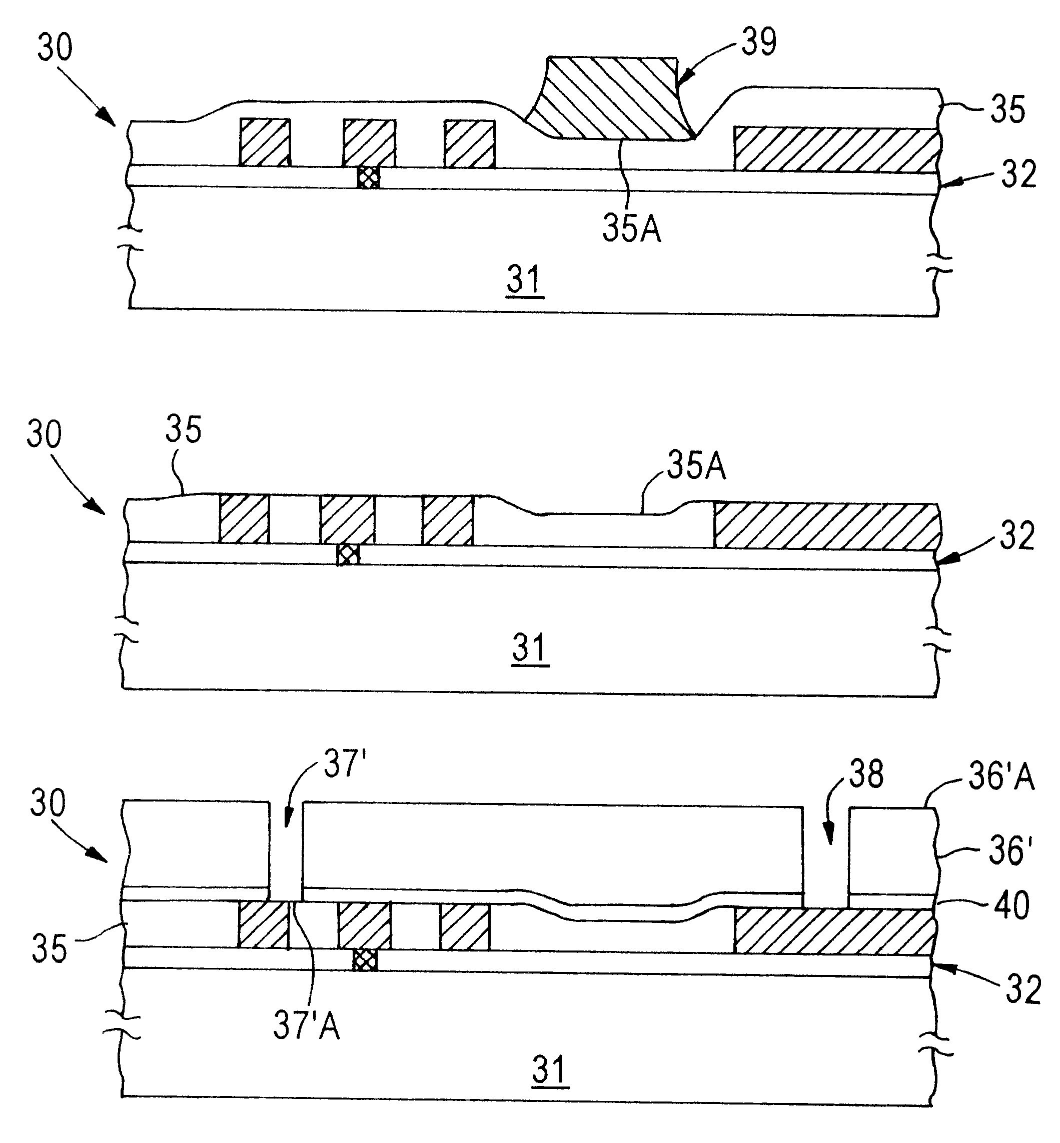
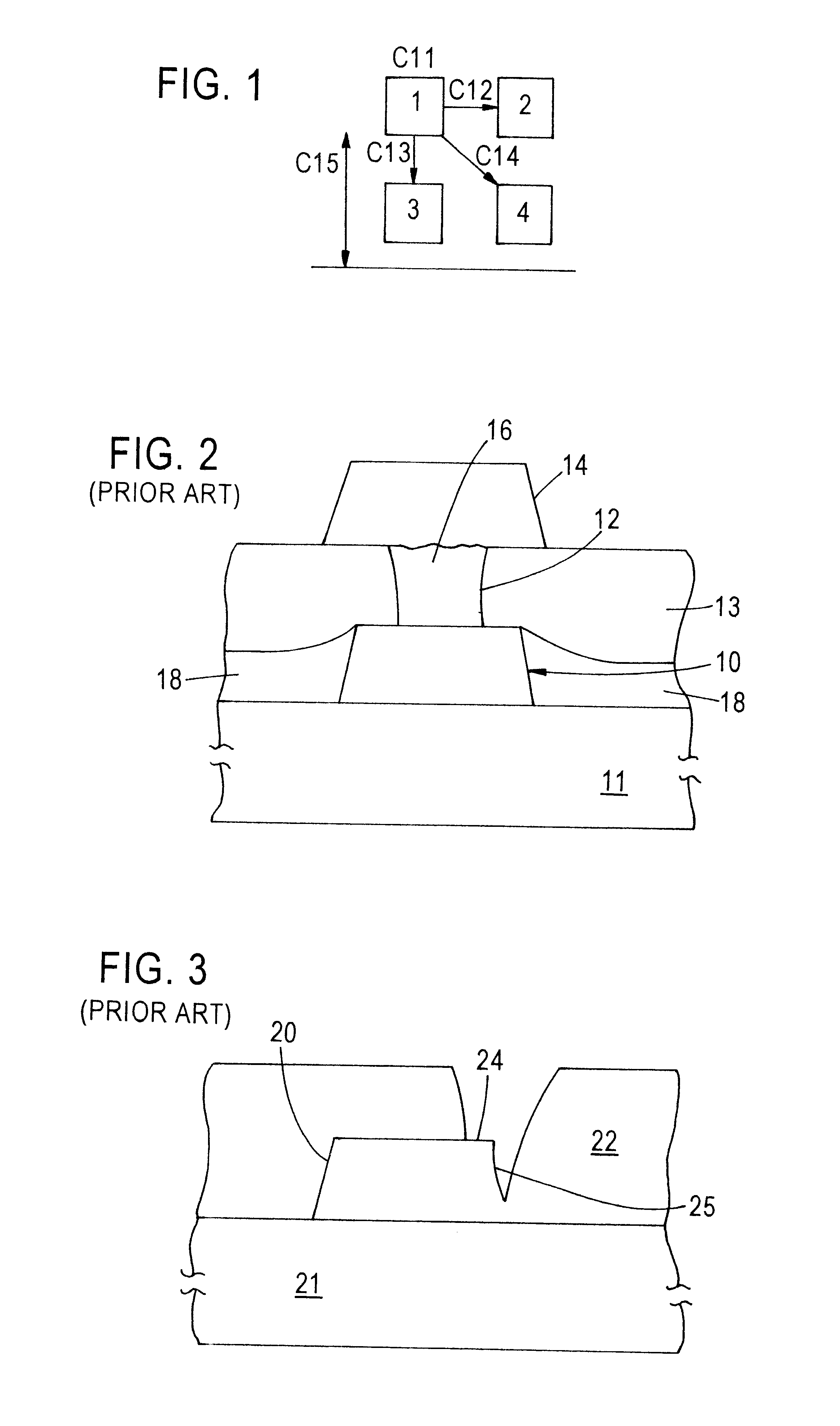
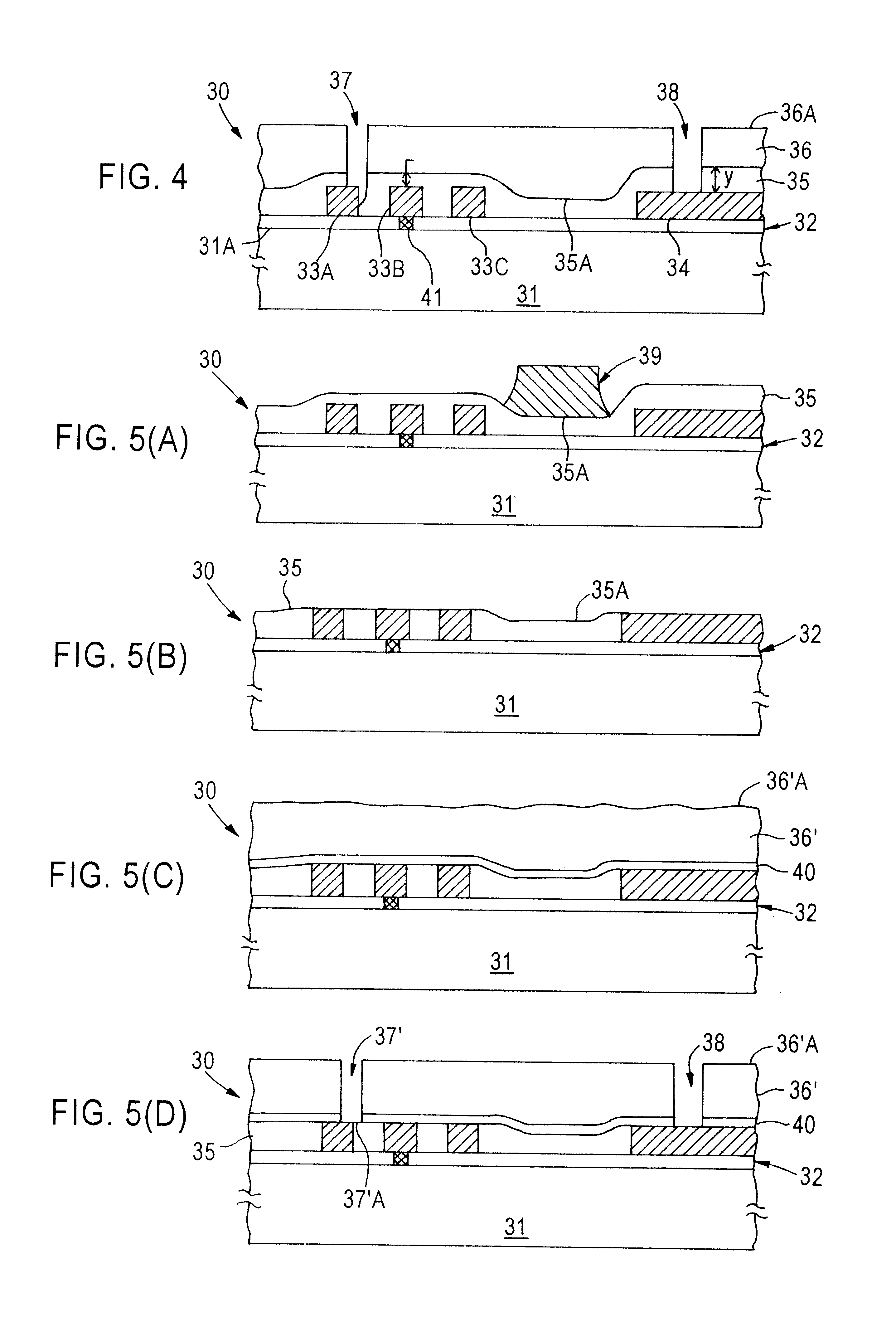
The present invention addresses and solves problems arising from manufacturing high-density integration, submicron-dimensioned, multi-metallization level semiconductor devices comprising in-laid "back-end" metallization patterns comprising a plurality of spaced-apart conductive features of varying dimensions and spacings, wherein, as part of the fabrication methodology, at least one via is formed in an interlayer dielectric layer, for electrically contacting at least one underlying electrically conductive feature formed on or within a dielectric layer formed on a surface of a semiconductor wafer substrate, the at least one conductive feature comprising an electrical contact area, interlevel metallization, and / or interconnection routing of at least one active device region or component formed on or within the semiconductor wafer substrate, and the at least one via comprising at least one borderless via.

Briefly stated, according to the present invention, problems of excessive variatio...


PUM


Abstract

Excessive variation in vertical (i.e., inter-level) capacitance of multi-level metallization semiconductor devices resulting in poor RC time constants of finished devices, and over-etching of borderless vias leading to inter-level short-circuits, are simultaneously eliminated or substantially reduced by selectively providing an etch-resistant masking material at thinner, i.e., recessed, portions of a first, low k gap fill material blanket-deposited over spaced-apart features of a metallization pattern and in the spaces therebetween. The surfaces of thicker, non-recessed portions thereof are etched so as to be substantially co-planar with the feature surfaces and the recessed portions. The etch-resistant mask is then removed, and second and third dielectric layers deposited over the planarized surface. The second and third dielectric layers are selected such that the second dielectric layer etches at a substantially slower rate than the third dielectric layer, thereby serving as a partial etch stop layer preventing deleterious over-etching of the borderless via.

Description

The present invention relates to the formation of high-density, multi-layer metallization semiconductor devices with reduced vertical capacitance variation. The invention has particular applicability in the manufacture of high-density, multi-layer metallization semiconductor devices with design features in the deep submicron range, such as 0.18 .mu.m and below, e.g., 0.15 .mu.m and below.The present invention relates to a method for forming semiconductor devices comprising multi-layer metallization systems with reduced vertical capacitance variation, and multi-layer metallization semiconductor devices obtained thereby. The present invention is especially adapted for use in semiconductor device manufacturing processing employing "damascene" (or "in-laid") technology.The escalating requirements for high density and performance associated with ultra-large scale integration (ULSI) semiconductor device wiring are difficult to satisfy in terms of providing submicron-dimensioned (such as 0...

Claims


Application Information

Patent Timeline
Patent Type & Authority Patents(United States)
IPC IPC(8): H01L21/70H01L21/768H01L21/02H01L21/3105
CPCH01L21/31058H01L21/76834H01L21/76819H01L21/76802
Inventor CHEN, SUSAN H.BESSER, PAUL R.
Owner ADVANCED MICRO DEVICES INC
Why Eureka
Try Eureka