Thin film transistor including an amorphous layer and a high-defect density layer

a thin film transistor and defect density technology, applied in the field can solve the problems of large defect density of a-si film, and achieve the effect of high tft characteristic and increased productivity of thin film transistors

Inactive Publication Date: 2003-02-25
AU OPTRONICS CORP
View PDF7 Cites 26 Cited by
  • Summary
  • Abstract
  • Description
  • Claims
  • Application Information

AI Technical Summary

Benefits of technology

is to increase productivity of a thin film transistor and to produce a high TFT characterist...

Problems solved by technology

However, according to these background arts, although the film growth time can surely be shortened, the prior arts are nothing else more than preventing the deterioration of the TFT characteristic such as an electrical ...

Method used


Image

  • Thin film transistor including an amorphous layer and a high-defect density layer
  • Thin film transistor including an amorphous layer and a high-defect density layer
  • Thin film transistor including an amorphous layer and a high-defect density layer

Examples


an embodiment 1

of the present invention will be described with reference to the accompanying drawing in detail.

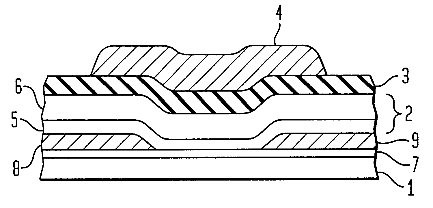
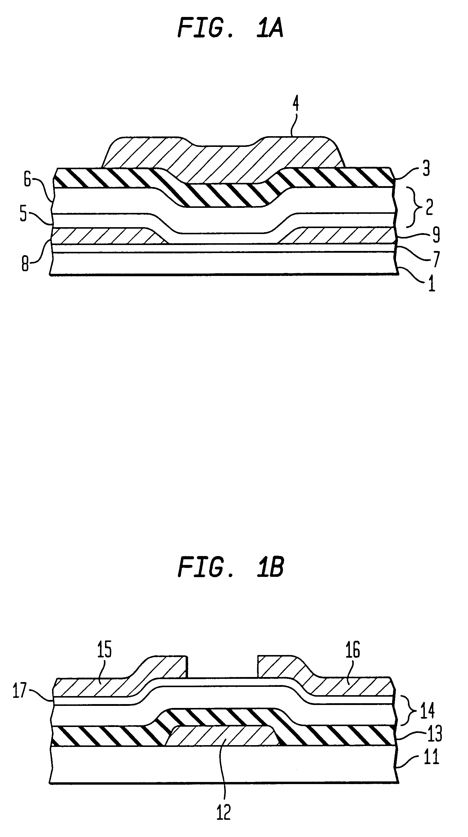
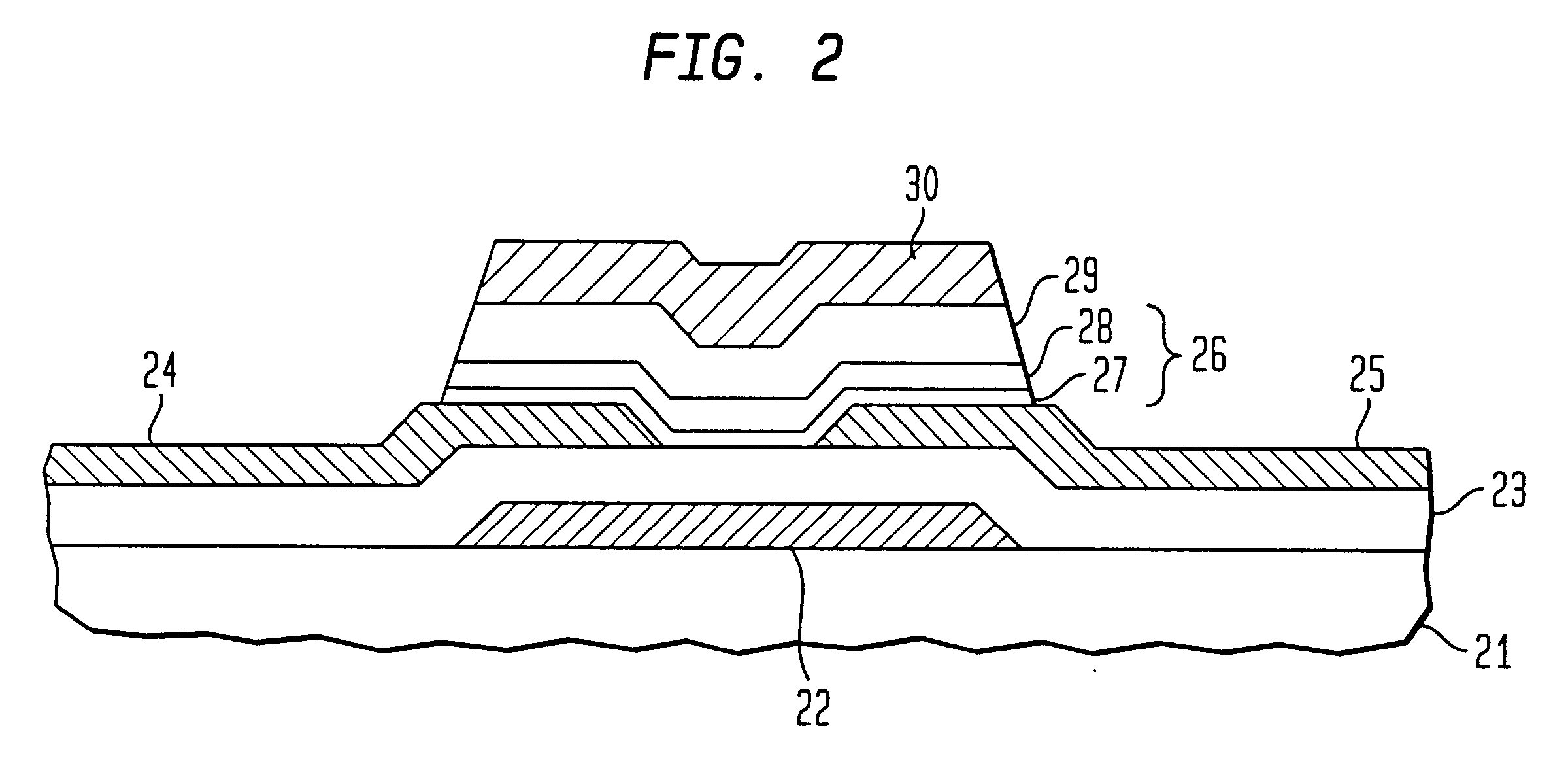
FIG. 2 is an explanatory view showing a structure of a thin film transistor in this embodiment 1. Specifically, FIG. 2 shows a top gate type (positive stagger) TFT structure. In FIG. 2, reference numeral 21 denotes an insulating substrate formed of no-alkali glass, quartz and the like. A light shield film 22 formed of Mo alloy such as Mo and MoCr is provided on the insulating substrate 21. An insulating film 23 formed of silicon oxide SiO.sub.X, silicon nitride SiN.sub.X and the like, which serves as an under coat layer, is provided so as to cover the upper portion of the light shield film 22. A pixel electrode (not shown) formed of an ITO (indium tin oxide) film, which is a transparent conductive film, is formed on the insulating film 23. Source and drain electrodes 24 and 25, which are formed integrally with the pixel electrode by laminating metal films such as molybdenum tungsten alloy...


PUM


Abstract

The present invention improves a productivity in growing an a-Si film in a thin film transistor and to obtain an excellent thin film transistor characteristic. More specifically, disclosed is a thin film transistor in which an amorphous silicon film 2, a gate insulating film 3 and a gate electrode are sequentially stacked on an insulating substrate 1. The amorphous silicon film 2 includes a low defect-density amorphous silicon layer 5 formed at a low deposition rate and a high deposition rate amorphous silicon layer 6 formed at a deposition rate higher than that of the low defect-density amorphous silicon layer 5. The low defect-density amorphous silicon layer 5 in the amorphous silicon film 2 is grown closer to the insulating substrate 1, and the high deposition rate amorphous silicon layer 6 is grown closer to the gate insulating film 3.

Description

1. Technical FieldThe present invention relates to a thin film transistor used for an active matrix liquid crystal display, a liquid crystal display device using the thin film transistor, and a method of fabricating the thin film transistor.2. Prior ArtA liquid display device employing an active matrix system, which uses a thin film transistor, comprises a TFT array substrate in which gate electrodes (Y-electrode) and data electrodes (X-electrode) are arranged in the form of a matrix and thin film transistors (TFT) are disposed at intersceting points of the matrix, and an opposite substrate located so as face the TFT array substrate with a space therebetween. By the thin film transistor, the liquid display device controls a voltage applied to a liquid crystal which is sealed between the TFT array substrate and the opposite substrate, and can performs a displaying utilizing an electro-optic effect of the liquid crystal.Here, as a structure of the thin film transistor (TFT), a top gat...

Claims


Application Information

Patent Timeline
IPC IPC(8): H01L21/02H01L29/66H01L21/336H01L29/786G02F1/136G02F1/1368H01L21/205
CPCH01L29/66765H01L29/78696H01L29/78669
Inventor TSUJIMURA, TAKATOSHITOKUHIRO, OSAMUMOROOKA, MITSUOMIYAMOTO, TAKASHI
Owner AU OPTRONICS CORP
Why Eureka
Try Eureka