Method for producing a tin-nickel alloy film
a technology of tin-nickel alloy and tin-nickel alloy, which is applied in the direction of metal-working apparatus, metal-layered products, decorative surface effects, etc., can solve the problems of restricted chemical species to be used, strict use restrictions, and increased use restrictions of chromium plating films
- Summary
- Abstract
- Description
- Claims
- Application Information
AI Technical Summary
Benefits of technology
Problems solved by technology
Method used
Image
Examples
example 1
A pure iron plate having a thickness of 2 mm as a substrate was immersed into a watts nickel bath having a total amount of 300 ml which was composed of 15 g of nickel chloride-hexahydrate, 90 g of nickel sulphate and 12 g of boric acid, and the watts nickel bath was electrolyzed by flowing a current at a current density of 5 A / dm.sup.2 for five minutes to form a nickel layer in a thickness of 30 .mu.m.
Then, the iron plate having the nickel layer thereon was immersed into a fluoroboric acidic bath having a total amount of 300 ml which was composed of 18 ml of 42%-boric hydrofluoric acid, 2 ml of 44.6%-fluoroboric tin and 15 mg of polyethylene glycol (molecular weight=2000). Then, the fluoroboric acidic bath was electrolyzed by flowing a current at a current density of 1 A / dm.sup.2 for five minutes to form a tin layer in a thickness of 30 .mu.m on the nickel layer and form a multi-layered film composed of the tin layer and the nickel layer.
example 2
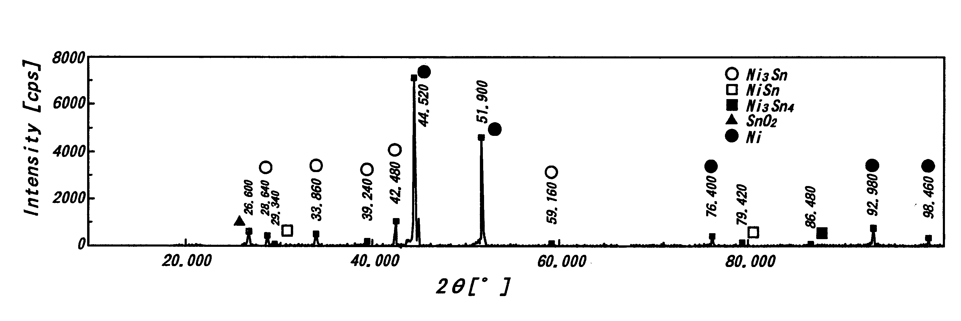
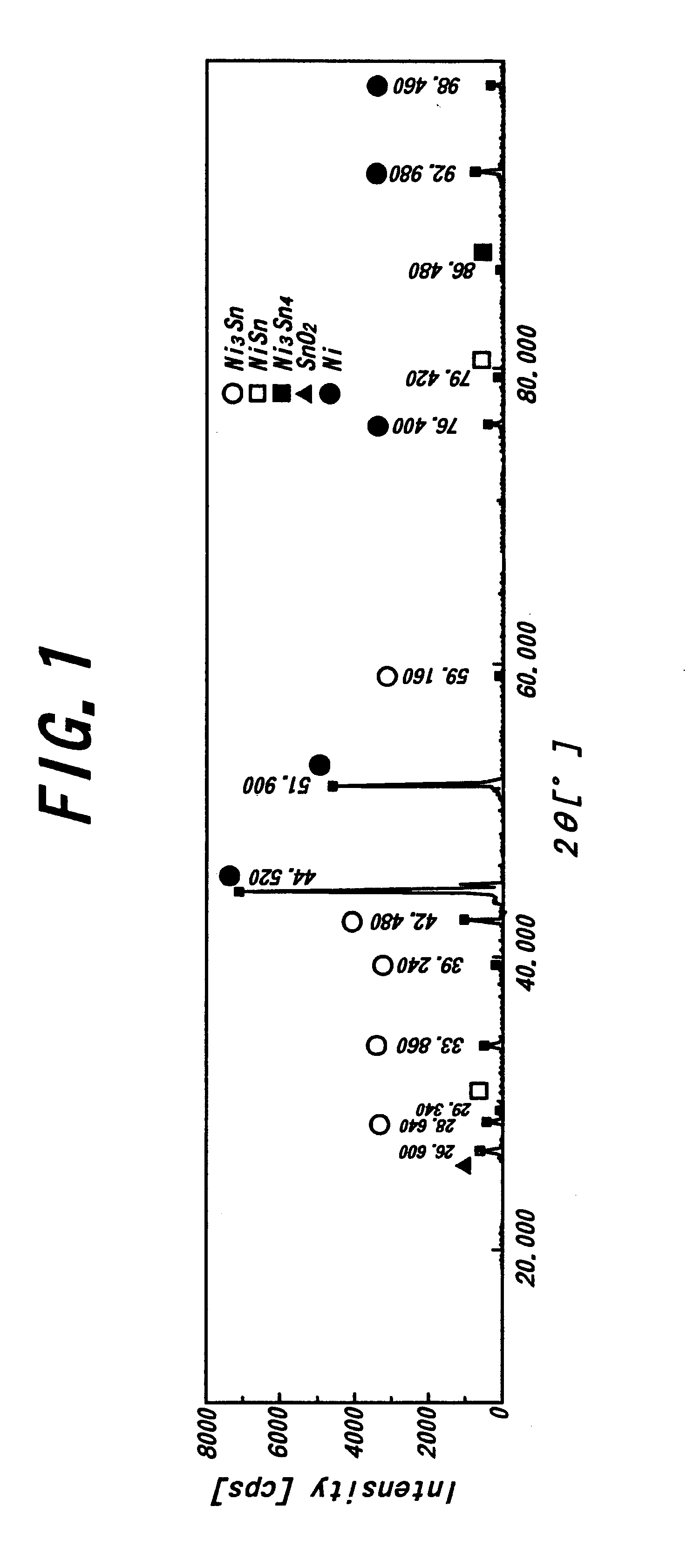
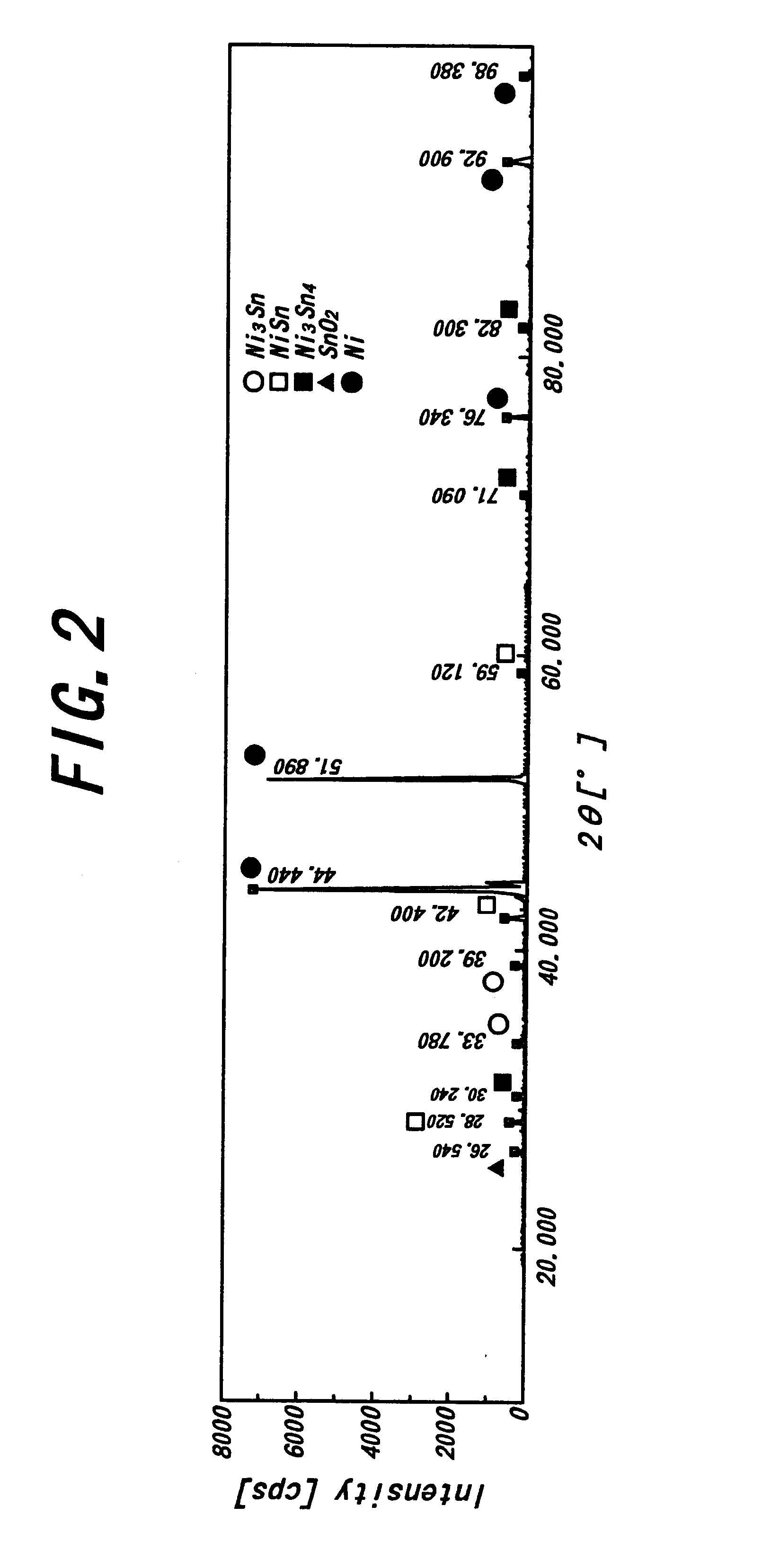
After the multi-layered film, in which the nickel layer and the tin layer are stacked in turn as in Example 1, was formed, laser beams having an intensity of 200 W / cm.sup.2 were irradiated onto the multi-layered film for 60 seconds from the CO.sub.2 laser, and thus, a tin-nickel alloy film was produced.
As a result, according to the present invention, the long time-reliable tin-nickel alloy film, not almost including the non-equilibrium NiSn phase, can be obtained in a short time.
Moreover, the above phenomenon was observed by an electron beam microanalyzer built-in a scanning microscope.
PUM
| Property | Measurement | Unit |
|---|---|---|
| thickness | aaaaa | aaaaa |
| boiling point | aaaaa | aaaaa |
| melting point | aaaaa | aaaaa |
Abstract
Description
Claims
Application Information


