Welding method for semiconductor materials

Inactive Publication Date: 2003-06-03
KOMATSU LTD
View PDF4 Cites 22 Cited by
  • Summary
  • Abstract
  • Description
  • Claims
  • Application Information

AI Technical Summary

Benefits of technology

For preventing contamination of the welding portion by metal or oxidation, void-free welding using electron beams or laser beams is achieved by degassing of a molten pool utilizing the periodical deflection of the heat source (zone). Moreover, by welding under decreased pressure, favorable welding of good quality is performed by further aiding prevention of oxidation and contamination.
As described so far, the present invention performs welding of semiconductor materials such as Si which was considered to be impossible to weld due to their very brittle characteristics. The welding is achieved by utilizing a heat source of high energy density, to permit welding of members made of semiconductor materials such as Si which could heretofore be manufactured only through mechanical processing. In addition, the present invention permits manufacturing of members having shapes which could not be obtained through mechanical processing. Consequently, the degree of freedom for processing semiconductor materials is remarkably improved.
In highly brittle materials s

Problems solved by technology

Adequate control during partial melting of members to be welded is difficult using ordinary type heat sources of low energy density.
This produces such a large h

Method used


Image

  • Welding method for semiconductor materials
  • Welding method for semiconductor materials
  • Welding method for semiconductor materials

Examples


Example

Embodiment 1

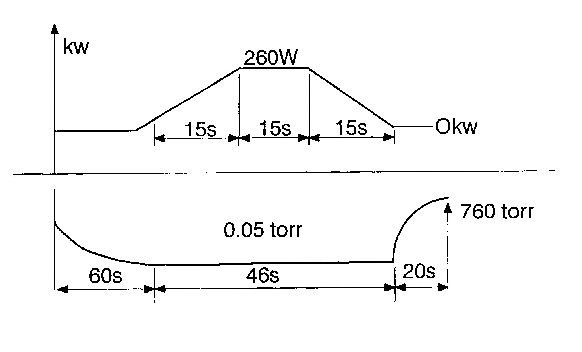
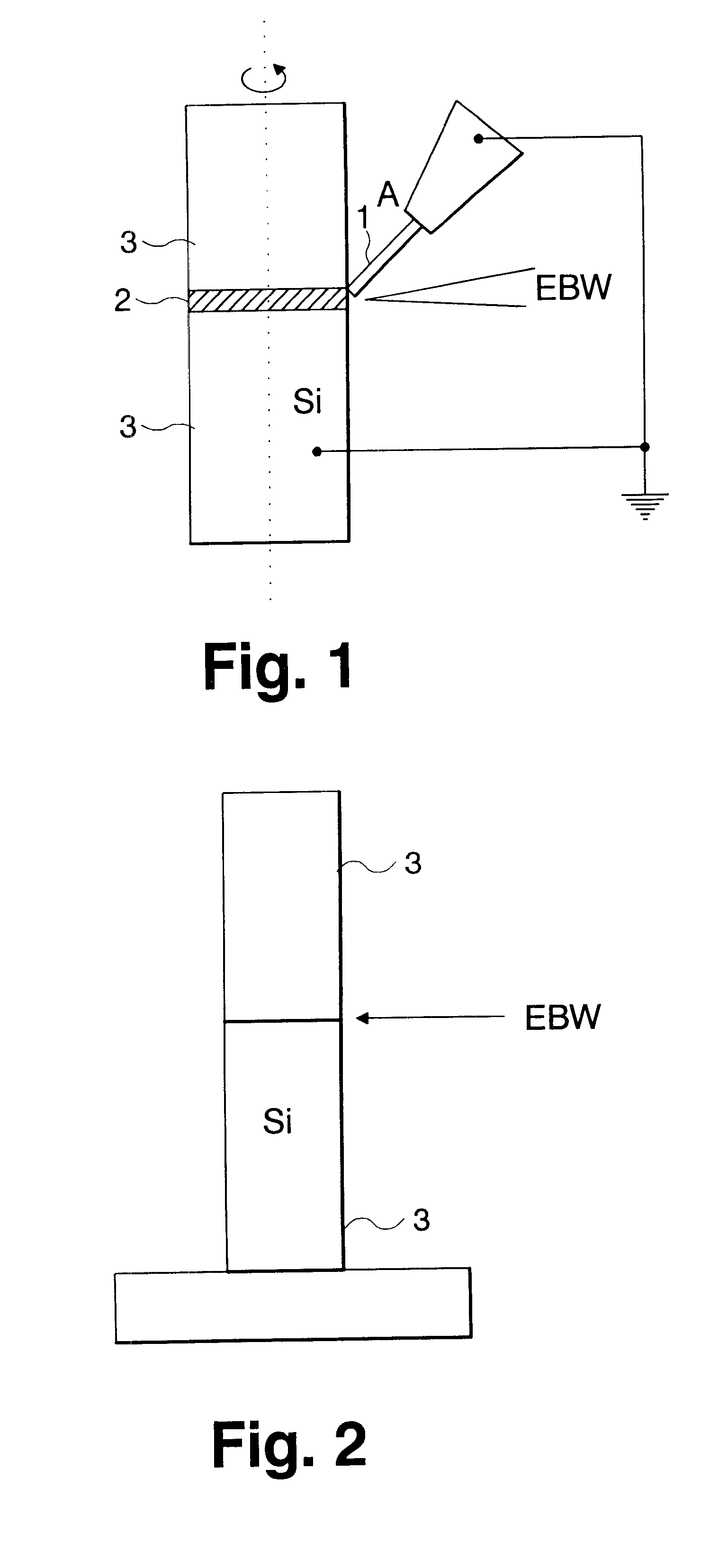
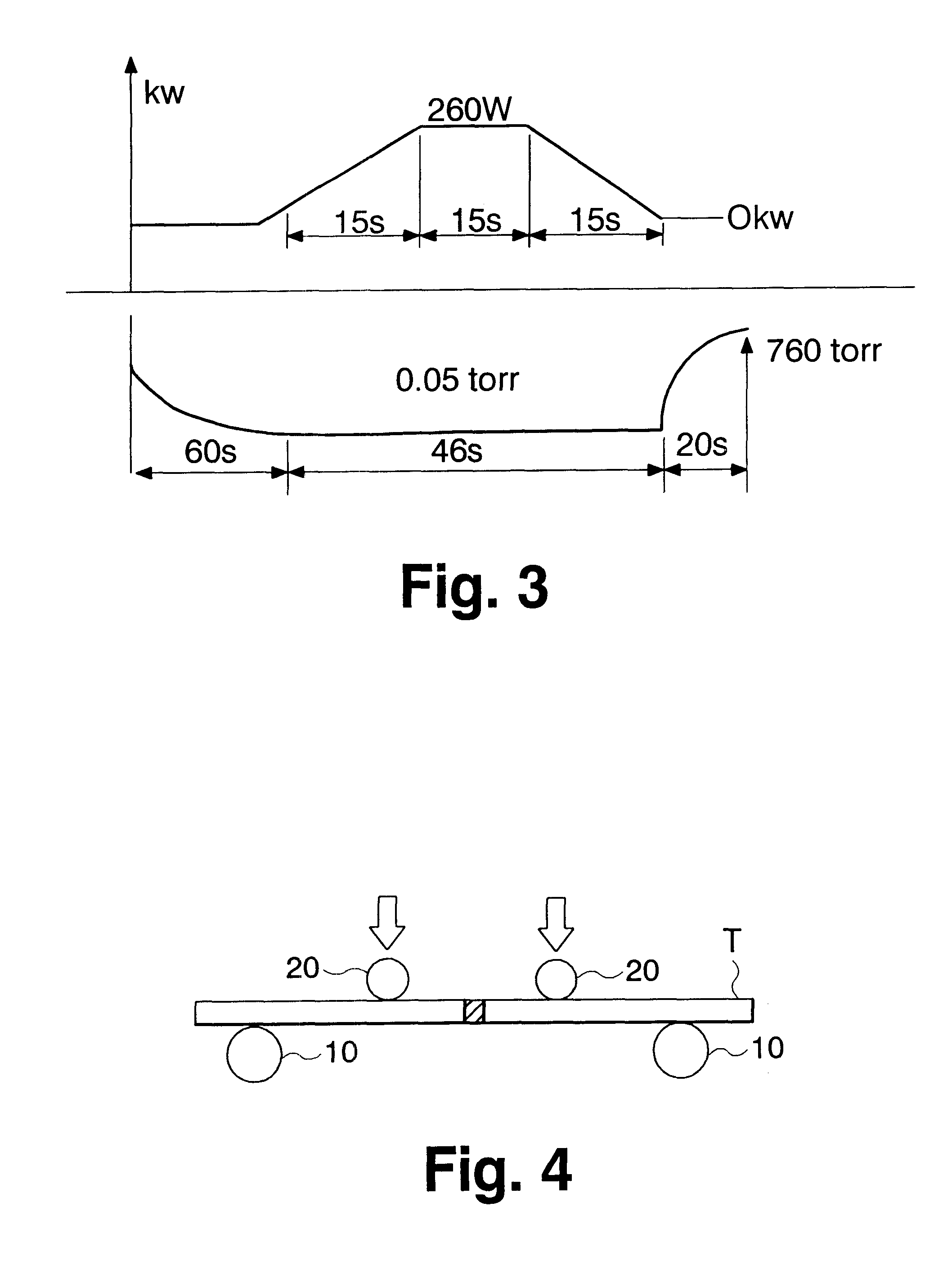
Referring to FIG. 2, single crystal Si members 3, 3, having a diameter of 8 mm were laterally overlapped. Electron beam welding was performed from a horizontal direction directed to the overlapped portion. First, tack welding was performed through two-point welding. After confirming that the overlapped Si members 3, 3 were unable to shift, electron beam welding was performed over the whole circumference while rotating the work. The clearance of the welding portion is set to be 0.5 to 1 mm. The welding conditions were set to achieve an acceleration voltage of 130 kv and a beam current of 5 mA. A rise time of 15 seconds were set to reach 5 mA at the starting welding. A descending time of 15 seconds from 5 mA was set at the terminating welding. The atmospheric pressure was maintained at not more than 0.05 Torr. It should be noted that while it is possible to perform welding with a clearance of not more than 1 mm between contact surfaces before welding, it is preferable that...

Example

Embodiment 2

It has been confirmed of effects of controlling the decrement of energy output during the termination welding in the above described Embodiment 1. The results thereof are shown in FIG. 7. FIG. 7(a) shows a sectional shape of a bead at an end portion obtained in the above described Embodiment 1. FIG. 7(b) shows a sectional shape of a bead at an end portion of which no decrement control was performed. As is clear from the drawings, protrusions P in FIG. 7(b) are formed due to directional solidification which is a characteristic of Si in the absence of decrement control. However, in case decrement control has been performed, the molten pool is controlled in a gradually decreasing manner so that forming of protrusions is remarkably restricted, as shown in FIG. 7(a). By eliminating discontinuities in shape in this manner, the welding strength is improved.

Example

Embodiment 3

Referring now to FIG. 8, another embodiment of the invention includes changing the shape of the . In this embodiment, polycrystal Si members 3, 3 having a diameter of 6 mm are crossed at 90 degrees and are welded. In this coupling, joining surfaces were cut to 45 degrees and fixed facing each and fixed in position by ajig. The clearance between the members 3, 3 is set to be 0.5 to 1 mm. Then, welding was performed by spot irradiation of electron beams along the overlapping surface as shown in the drawings. The welding conditions are identical with those as shown in FIG. 3. While couplings assume different shapes at their welding portions after welding which are due to directional differences of the gravity head actuating on the molten pool when irradiation of the electron beam is performed in a horizontal direction and when irradiation is performed in a vertical direction, both methods are effective in obtaining favorable couplings.


PUM

PropertyMeasurementUnit
Timeaaaaaaaaaa
Pressureaaaaaaaaaa
Angleaaaaaaaaaa

Abstract

Two overlapped semiconductor materials are welded by a melt welding under the influence of a heat source of high energy density. The energy output of the heat source is ramped up slowly at the beginning of welding and ramped down slowly at completion of welding. In one embodiment the semiconductor materials are preheated before welding. In another embodiment, the effective position of the heat source on the semiconductor materials is periodically deflected.

Description

1. Field of the InventionThe present invention relates to a welding method for a semiconductor material such as single crystal or polycrystal silicon (hereinafter referred to as "Si"), gallium (hereinafter referred to as "Ga") or arsenic (hereinafter referred to as "As"), wherein the semiconductor materials are welded by means such as electron beam, laser beam, or arc.2. Description of the Related Art,The physical and electrical properties of Si, when used as a semiconductor, have made it very popular. Si is especially utilized as a bulk material for substrates of DRAMs (Direct Random Access Memories) or MPUs (Micro Processor Units). The demand therefor is growing mostly for use as wafers. The diameters of wafers are becoming larger in order to produce more circuits in a single operation. Si ingots, of which wafers are made, currently exceed 200 kg in weight. As a consequence of this weight, it is necessary to consider how to hold and transport such ingots during subsequent manufact...

Claims


Application Information

Patent Timeline
IPC IPC(8): B23K26/32B23K26/00C30B33/00C30B33/06B23K15/00B23K101/40H01L21/18H01L21/263H01L21/302H01L21/58
CPCC30B33/06H01L21/185H01L21/2636H01L21/302H01L24/26H01L24/83H01L2924/01033H01L2224/8319H01L2224/8385H01L2924/01004H01L2924/01005H01L2924/01015H01L2924/07802H01L2924/01006H01L2924/3512H01L2924/00H01L2224/83048H01L2924/351
Inventor KURIYAMA, KAZUYAHANADA, YOICHIRO
Owner KOMATSU LTD
Why Eureka
Try Eureka