Electronic device and manufacture thereof

a technology of electronic devices and components, applied in the field of electronic components, can solve the problems of insufficient high-frequency stable operation, large mounting boards, and limited conventional methods, and achieve the effects of convenient and efficient operation, simplified apparatus, and efficient hole formation

Inactive Publication Date: 2003-06-03
PANASONIC CORP
View PDF7 Cites 8 Cited by
  • Summary
  • Abstract
  • Description
  • Claims
  • Application Information

AI Technical Summary

Benefits of technology

In the above-described method for manufacturing the electronic component of the third configuration of the present invention, the patterned metal thin film can be formed by forming the metal thin film after applying a solid mask or an evaporative mask, or by forming the metal thin film followed by a laser etching. With this configuration, the metal thin film with a desired shape can be obtained easily and efficiently.
Next, a method for manufacturing the electronic component according to the fourth configuration of the present invention includes obtaining a layered product by a plurality of times of depositing a metal thin film that is patterned in a predetermined shape and a dielectric thin film, forming a hole in the layered product in a deposition direction, and filling a conductive substance in the hole. With this configuration, an opening is not formed in the dielectric thin film while manufacturing the layered product and a hole is formed after obtaining the layered product, thereby simplifying the apparatus for manufacturing the layered product.
In the above-described method for manufacturing the electronic component of the fourth configuration of the present invention, the hole can be a penetrating hole that is formed so as not to penetrate said metal thin films. Thus, the penetrating electrode can be formed easily.
Also, a plurality of layers of the metal thin film are formed and the hole is formed so that a part of the metal thin films is exposed to an inner wall of the hole. Then, filling the conductive substance so as to be connected to the exposed metal thin film can form a lead electrode easily. It is possible for the hole here to penetrate or not to penetrate the electronic component.
In the above-described method for manufacturing the electronic component of the fourth configuration of the present invention, it is preferable that the hole is formed by irradiating a laser beam. With this configuration, the hole can be formed efficiently. The laser beam source used here is preferably selected considering whether or not it penetrates the metal thin film layers at the same time.

Problems solved by technology

Conventional methods are limited to those of forming a minute capacitor inside the semiconductor, and this is becoming insufficient for a further high-frequency stable operation.
In addition, locating the capacitor in the circumference of the semiconductor chip causes a problem in that a mounted board becomes large.

Method used


Image

  • Electronic device and manufacture thereof
  • Electronic device and manufacture thereof
  • Electronic device and manufacture thereof

Examples


second embodiment

(Second Embodiment)

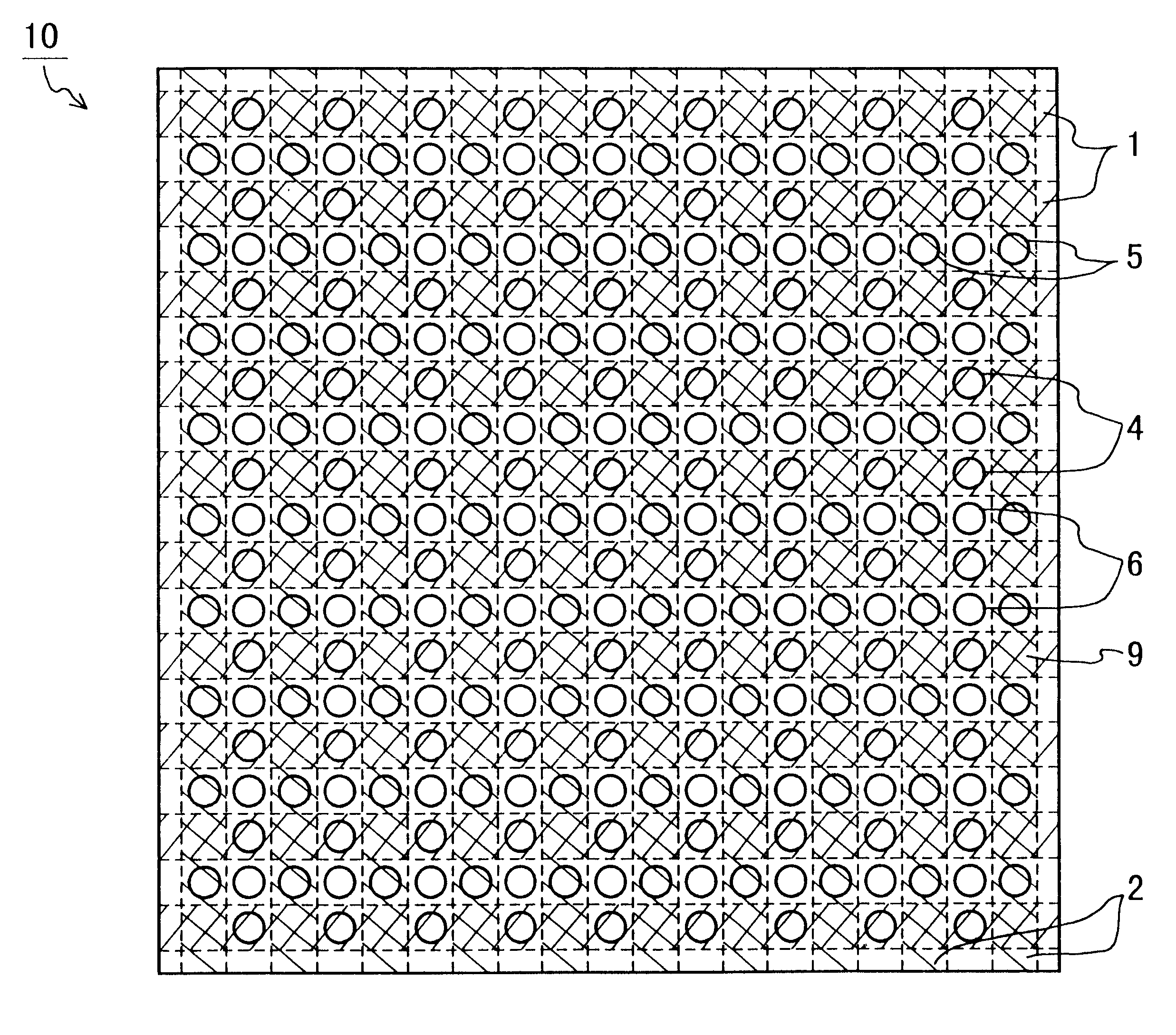
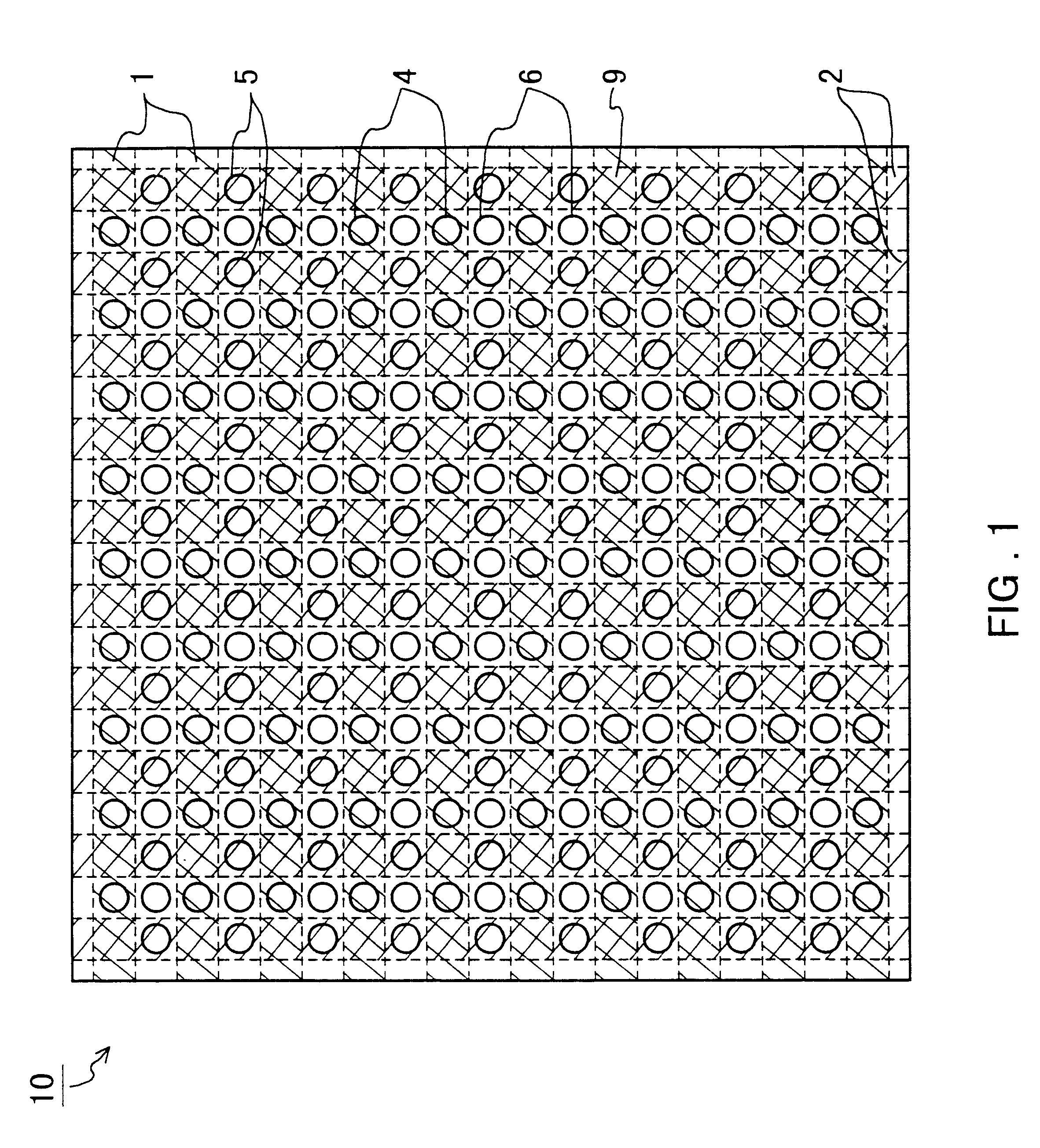
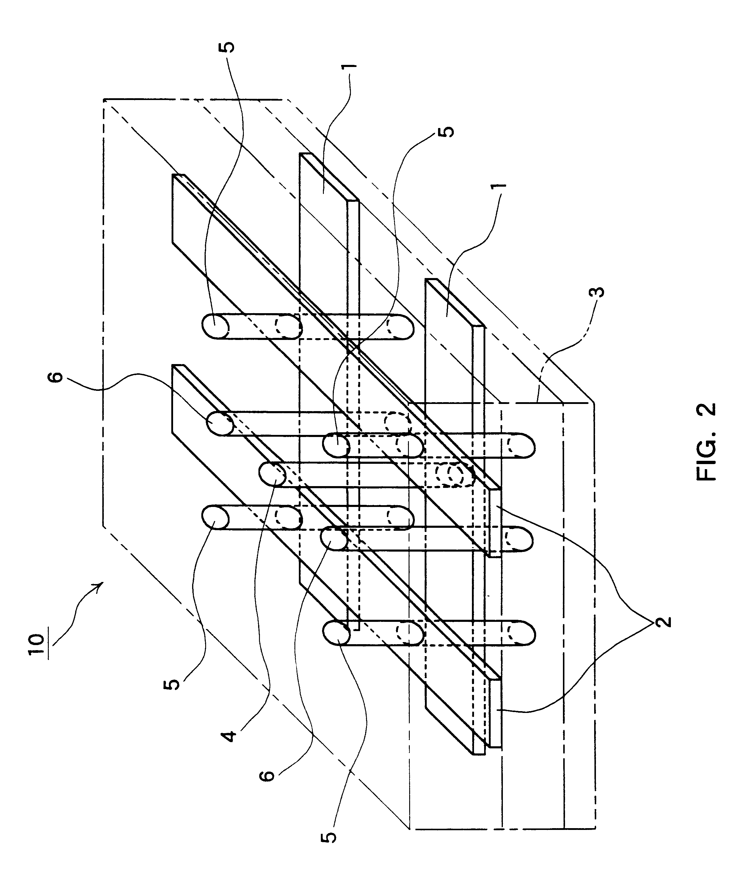
FIG. 5 is a schematic plan view showing another example of the electronic component 10 according to the second embodiment of the present invention. FIG. 6 is a perspective view showing an internal structure of a part of the electronic component of FIG. 5.

A plurality of first electrode layers 1 are formed so as to be stripe-shaped on substantially the same plane, and a plurality of second electrode layers 2 are formed so as to be stripe-shaped on substantially the same plane. They are layered so that a dielectric layer 3 is interposed between the first electrode layers 1 and the second electrode layers 2. By crossing the directions of the stripes of the first electrode layers 1 and the second electrode layers 2, capacitance forming regions 9 are formed at the intersections and function as capacitors.

External electrodes 7 and 8 are formed on the peripheral surfaces of the electronic component 10. A first external electrode 7 is connected to the first electrode layer...

example 2

Aluminum was used as a metal thin film material, acrylate was used as a dielectric material, and silver-based paste was used as a conductive paste. For forming holes for penetrating electrodes in the dielectric layer, the following method was adopted. The method includes removing dielectric in a predetermined portion by laser etching after forming the dielectric layer. A carbon dioxide gas laser with an output of 10 W was used as the laser. Within an area 17 mm square, 484 penetrating electrodes with a diameter of 0.25 mm were formed on 0.8 mm-pitch lattice points. The electrode layers 1 and 2 were both 0.8 mm-wide multiple stripes. Depositing the electrode layer with a thickness of 30 nm and the dielectric layer with a thickness of 0.25 .mu.m was repeated so as to obtain 140 dielectric layers. Insulator layers with a thickness of 5 .mu.m respectively were formed on the upper and lower sides of the layered product to improve its strength. The upper and lower insulator layers were ma...

third embodiment

(Third Embodiment)

FIG. 9 is a schematic plan view showing an example of an electronic component 10 according to the third embodiment of the present invention. FIG. 10 is a perspective view showing an internal structure of a part of the electronic component of FIG. 9.

A plurality of first electrode layers 1 are formed in a predetermined pattern in substantially the same plane, and a plurality of second electrode layers 2 are formed in a predetermined pattern in substantially the same plane. They are layered so that a dielectric layer 3 is interposed between the first electrode layers 1 and the second electrode layers 2. By forming the first electrode layer 1 and the second electrode layer 2 so that at least a part of them overlap (face) each other, capacitance forming regions 9 are formed at the overlapped portions (facing portions) and function as capacitors. The capacitance can be changed by adjusting the size of each overlapped portion (the capacitance forming region 9).

A first lea...


PUM


Abstract

Electrode layers (1, 2) are arranged on both sides of a dielectric layer (3) facing each other so as to configure a capacitor. Lead electrodes (4, 5) are formed in the electrode layers (1, 2). A penetrating electrode (6) that is insulated from the electrode layers (1, 2) is formed. An electronic component (10) configured in this manner is mounted on a wiring board, and a semiconductor chip can be mounted thereon. Along with connecting the semiconductor chip to the wiring board via the penetrating electrode (6), the semiconductor chip or the wiring board is connected to the lead electrodes (4, 5). In this manner, while suppressing the size increase of a mounted area, the capacitor or the like can be arranged near the semiconductor chip. Thus, the semiconductor chip is driven with high frequency more easily.

Description

The present invention relates to an electronic component and a method for manufacturing the same.The request for speeding up information processing has become more and more intensified, and a growing number of semiconductor chips with high frequency have been developed year by year. In order to speed up the semiconductor operation, not only achieving high density and high performance of integrated chips but also improving characteristics of peripheral circuits is necessary. In particular, securing the stability of a transmission line and a power supply line is one of the requirements for the stable high-speed operation. Thus, it is not going too far to say that the main body of a semiconductor chip depends heavily on the peripheral devices.A capacitor is one of the important devices that secure the stability of the transmission line and the power supply line. In order to realize the high-speed operation, not only should the capacitor have high frequency performance, but also the wir...

Claims


Application Information

Patent Timeline
Patent Type & Authority Patents(United States)
IPC IPC(8): H01L23/48H01L23/50H01L23/498H05K1/16H05K3/40H05K1/00H05K3/46H05K1/14H05K1/02H01G4/30H01G4/33H01G4/38H01L21/822H01L27/04H05K3/00
CPCH01G4/33H01L23/49827H01L23/50H05K1/162H01L23/49822H01L2224/16H01L2924/15311H01L2924/3011H05K1/0231H05K1/0289H05K1/141H05K3/0026H05K3/403H05K3/467H05K2201/0179H05K2201/049H05K2201/09236H05K2201/10734H01G4/38
Inventor HONDA, KAZUYOSHIECHIGO, NORIYASUODAGIRI, MASARUSUGIMOTO, TAKANORI
Owner PANASONIC CORP
Why Eureka
Try Eureka