
Approach to structurally reinforcing the mechanical performance of silicon level interconnect layers

a technology of interconnect layers and mechanical properties, applied in the direction of semiconductor/solid-state device details, chemistry apparatus and processes, transportation and packaging, etc., can solve the problems of deformation of the underlying metal structure, delamination of the layers in the metal structure, and fracture of the underlying dielectri

Inactive Publication Date: 2003-07-01
TEXAS INSTR INC
View PDF6 Cites 26 Cited by
  • Summary
  • Abstract
  • Description
  • Claims
  • Application Information

AI Technical Summary

Problems solved by technology

A well known problem area in semiconductor processing is the process of attaching a solder, wire or other bonding elements to a bond pad on a semiconductor integrated circuit.
During the bonding process, mechanical loading and ultrasonic stresses applied by the bonding capillary tip to the bond pad often result in fracture of the underlying dielectrics, deformation of the underlying metal structures, and delamination of the layers in the metal structures.
These bonding failures may appear as craters in the bond pad and underlying layers as the bonding capillary tip is pulled away from the bonding pad.
However, these defects often are not apparent during bonding but would manifest themselves during subsequent bond pull and shear tests, reliability tests such as thermal cycle or thermal shock, or upon deprocessing and cross-sectioning.
Further, weakness of the bond pad structure may also reveal itself during wafer probing prior to bonding.
Again, the stresses exerted by the probe tips, typically formed of a hard metal such as tungsten and copper beryllium, can cause localized fractures in the pads, despite the fact that they make contact with softer metals such as aluminum and copper, on the bond pads.
Such fractures are as much of a reliability hazard as those caused during bonding.
Although general guidelines of parameter setpoints and configurations have been developed, the bonding failures persist at a sufficiently significant level to continually threaten the reliability of integrated circuit devices.
Yet the failure levels are low such that bonding failures become apparent only after several tens of thousands of devices are bonded.
Recent technological advances in semiconductor processing do not alleviate the situation.
New dielectric materials with lower dielectric constants are being used to increase circuit speeds but they are mechanically weaker than the conventional plasma enhanced chemical vapor deposition (CVD) dielectrics.
Inaccessibility of higher bond parameter settings for fear of damage to the bond pads also results in longer bond formation time, and consequently, lost throughput.
All these significant changes point to a trend of more severe failures and increase in their frequency.

Method used


Image

  • Approach to structurally reinforcing the mechanical performance of silicon level interconnect layers
  • Approach to structurally reinforcing the mechanical performance of silicon level interconnect layers
  • Approach to structurally reinforcing the mechanical performance of silicon level interconnect layers

Examples


Embodiment Construction

With the advancement of silicon technology in to newer process nodes, conventional probing and bonding techniques begin to create extensive mechanical damage in the form of micro-cracks under the bond pad areas. Micro-cracking can be more than a cosmetic problem. It can cause yield loss due to an electrical fail and / or affect device reliability. Micro-cracking in newer technologies is believed to be due to the use of a thinner top metal interconnect layer. In many cases, the thickness of the top metal interconnect is being reduced from around 6000 .ANG. to 4500-5000 .ANG.. These micro-cracks may result in significant yield loss after probe and / or wire bonding or flip-chip interconnect operations. The resulting level of yield loss and / or non-reliable products is expected to be 10-20%.

The problem is likely to be further compounded as low dielectric constant (low-k) materials are employed. The low-k materials are typically less mechanically durable. However, the low-k materials are nee...


PUM

PropertyMeasurementUnit
Dielectric polarization enthalpyaaaaaaaaaa
Electrical conductoraaaaaaaaaa
Stress concentration factoraaaaaaaaaa

Abstract

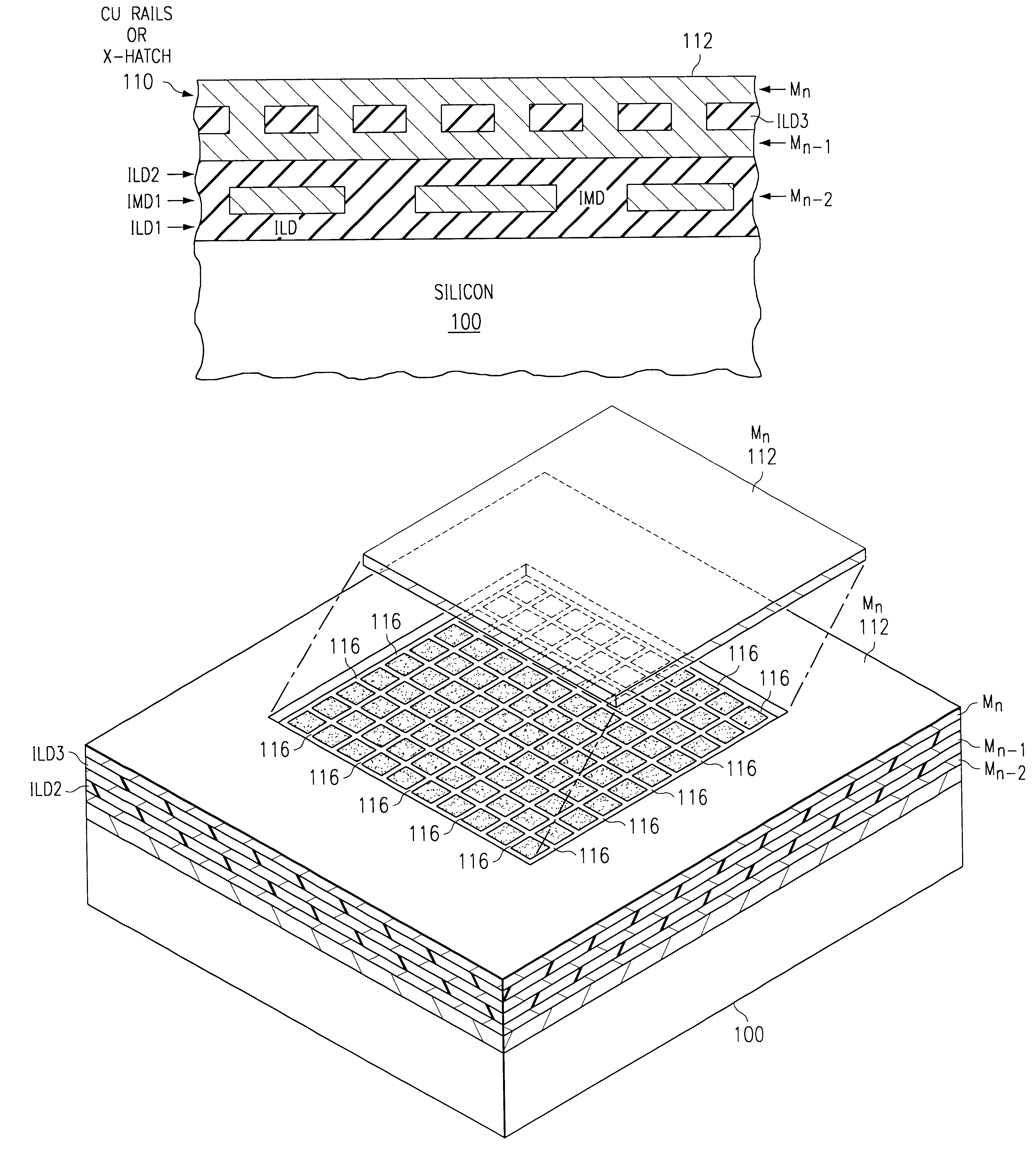
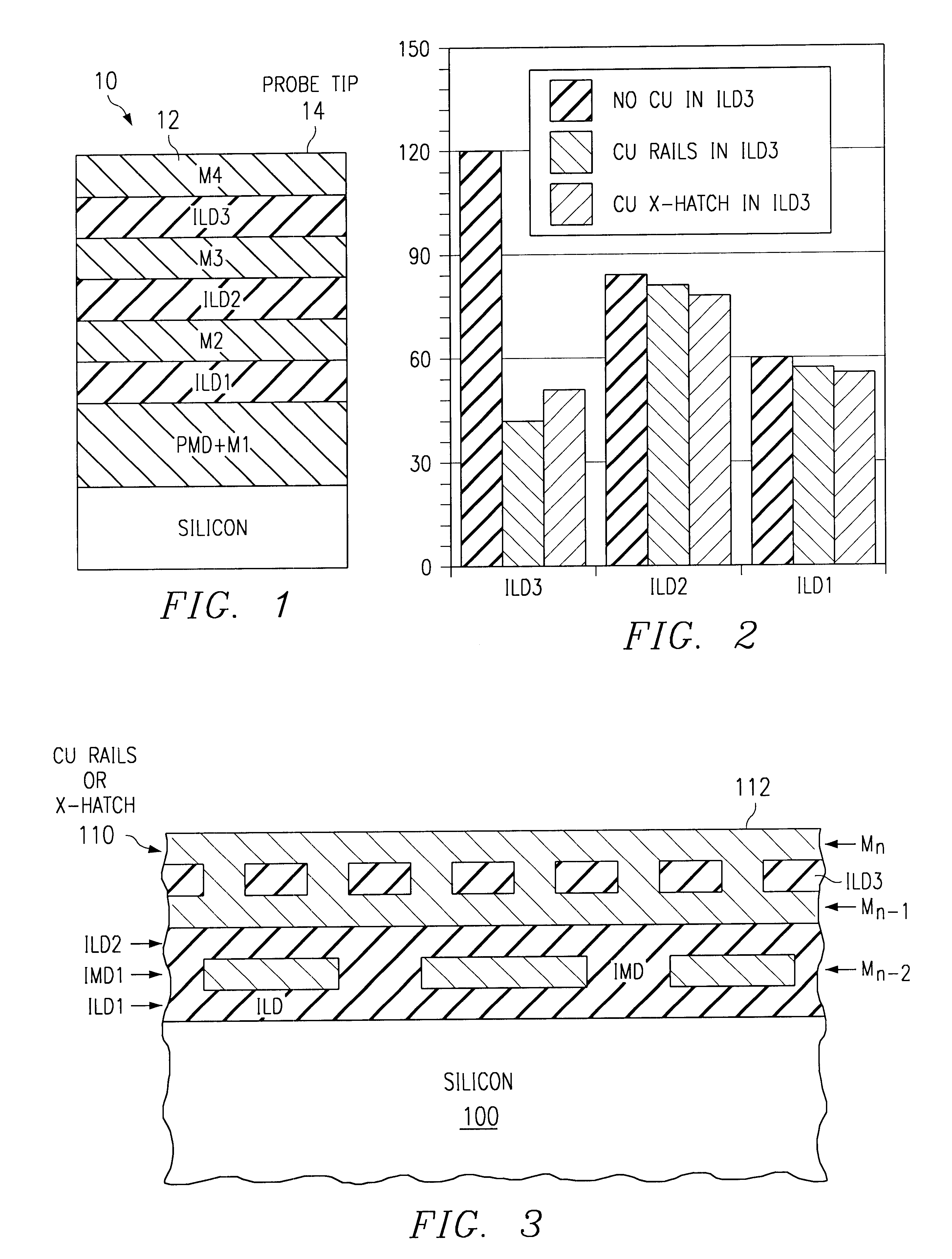
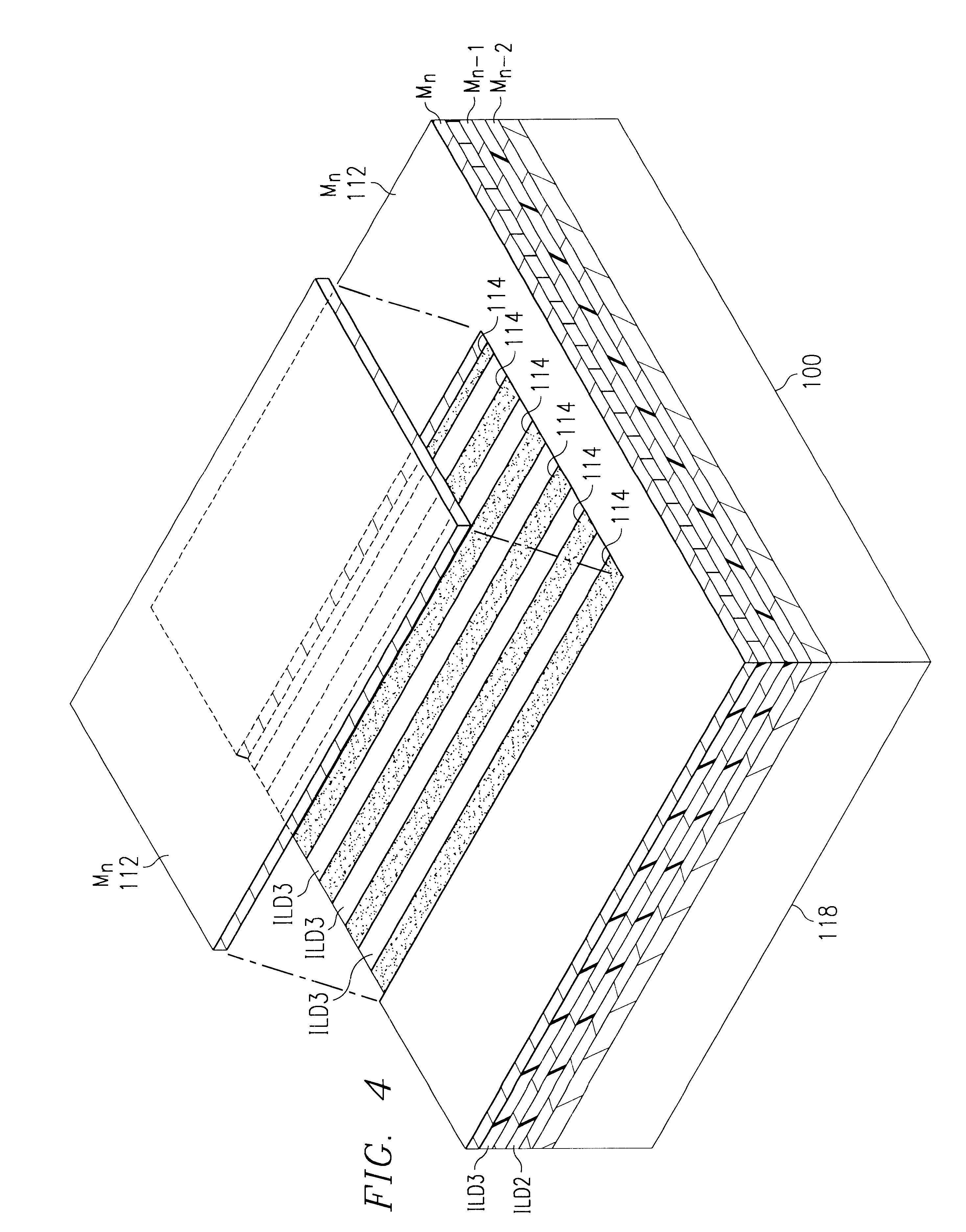
A conductive via pattern (110) between the uppermost metal interconnect layer (Mn) and next underlying metal interconnect layer (Mn-1) in the bond pad areas strengthens the interlevel dielectric (ILD3) between metal layers (Mn and Mn-1). The conductive via layer (110) may, for example, comprise parallel rails (114) or a grid of cross-hatch rails (116). By spreading the stress concentration laterally, the conductive via layer (110) inhibits micro-cracking from stress applied to the bond pad (112).

Description

The following co-pending U.S. patent application is believed to be relevant: Ser. No. 08 / 847,239 filed Apr. 30, 1997 to Saran et al, now U.S. Pat. No. 6,143,396.1. Field of the InventionThe invention is generally related to the field of integrated circuits and more specifically to improving the mechanical stability of interconnects under bond pads in an integrated circuit.2. Background of the InventionA well known problem area in semiconductor processing is the process of attaching a solder, wire or other bonding elements to a bond pad on a semiconductor integrated circuit. These bond pads are typically disposed above one or more layers or stacks of brittle and / or soft dielectric materials, typically oxides of silicon and some organic materials, for planarization and insulation purposes. Some dielectric materials, such as hydrogen silsesquioxane (HSQ), organo-silicate glass (OSG), aerogels, organic polyimides, parylenes, and others are advantageous for their low dielectric constants...

Claims


Application Information

Patent Timeline
IPC IPC(8): B32B15/04H01L23/48H01L23/485H01L21/3205H01L23/52H01L21/60
CPCB32B15/04H01L24/05H01L24/03Y10T428/24917H01L2924/01004H01L2924/01013H01L2924/01014H01L2924/01025H01L2924/01027H01L2924/01029H01L2924/01073H01L2924/01074H01L2924/01082H01L2924/014H01L2924/04953H01L2924/14H01L2924/01019H01L2924/01033H01L2924/00014H01L2224/05556
Inventor CHISHOLM, MICHAEL F.EDWARDS, DARVIN R.HOTCHKISS, GREGORY B.RINCON, REYNALDOSUNDARARAMAN, VISWANATHAN
Owner TEXAS INSTR INC
Learn More