Optical modulator

a technology of optical modulator and optical waveguide, applied in the field of fiber optics, can solve the problems of non-observation of signal electrical field, decreased modulation bandwidth, non-uniform electronic, etc., and achieve the effect of increasing the transmission speed of the system, increasing the distance of the transmitted signal, and reducing the size of the electro-optical modulator

Inactive Publication Date: 2003-07-29
SRICO
View PDF11 Cites 19 Cited by
  • Summary
  • Abstract
  • Description
  • Claims
  • Application Information

AI Technical Summary

Benefits of technology

It is the object of the present invention to increase the transmission speed of the system by adjusting the chirp of the device.
It is the object of the present invention to increase the distance of the transmitted signal by adjusting the chirp of the device.
It is the object of the present invention to reduce the size of the electro-optical modulator.
It is the object of the present invention to increase the manufacturing yield from a starting wafer as a result of its reduced size.
It is an object of the present invention to improve the overall device stability.

Problems solved by technology

Unfortunately, because the positive and negative electrodes carrying the electronic signal are arranged on the same face of the electro-optic crystal, the full effect of electronic signal electrical field is not experienced by the optical carrier.
Further, because the angular distribution of the electric field electronic signal is not uniform as it passes through the optical wave guide branches, the optical signal experiences a non-uniform electronic signal in each plane across (perpendicular to) the optical path in the optical wave guides.
Such electric field distortion in the optical waveguides leads to decreased modulation bandwidth.
This results in further distortion of the optical signal and decreased modulation bandwidth.
However, the electronic signal electrodes are placed on the same face of the optical waveguide substrate resulting in the less than optimal interaction of the electronic electric field with the optical signal noted above.

Method used


Image

  • Optical modulator
  • Optical modulator
  • Optical modulator

Examples


Embodiment Construction

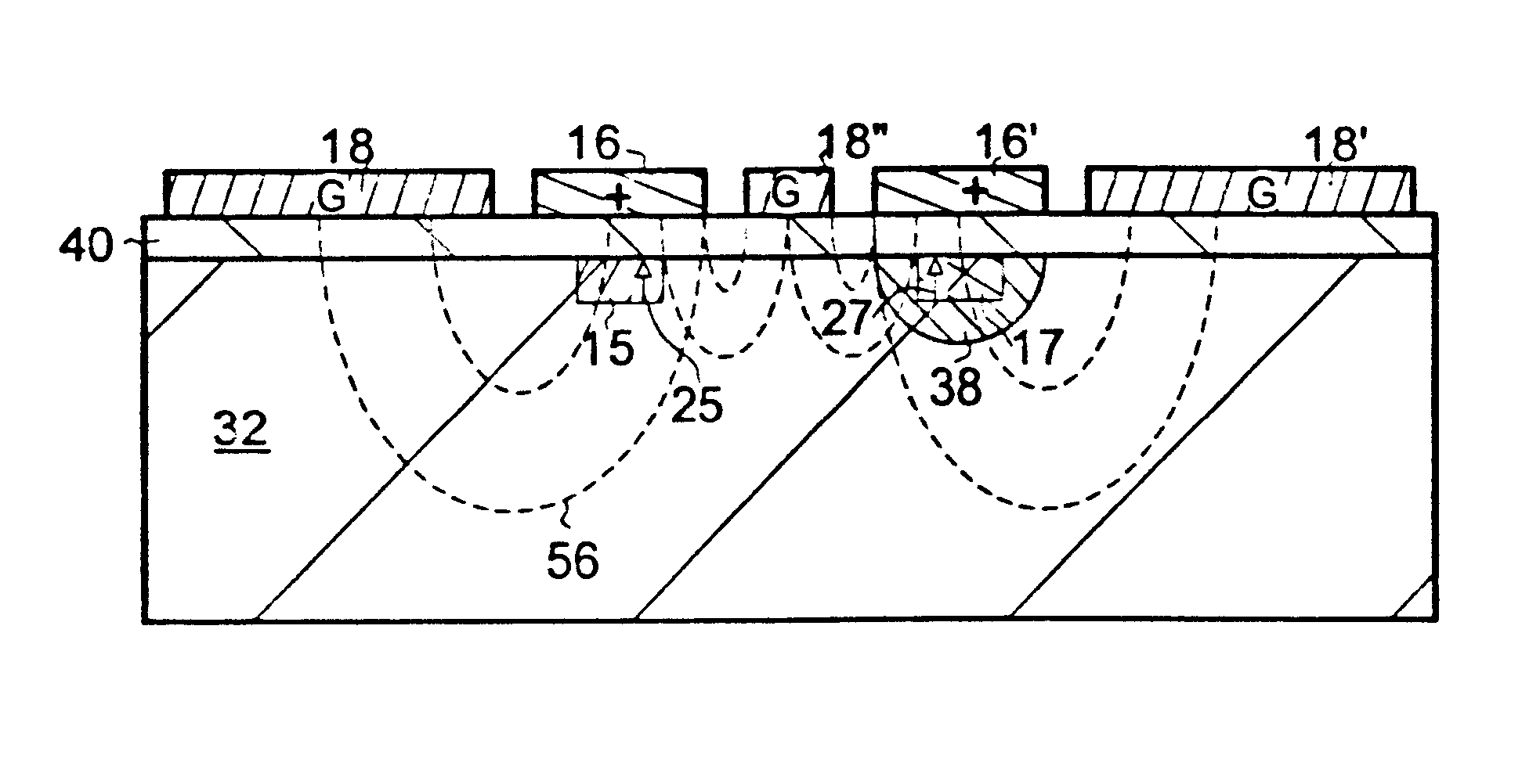
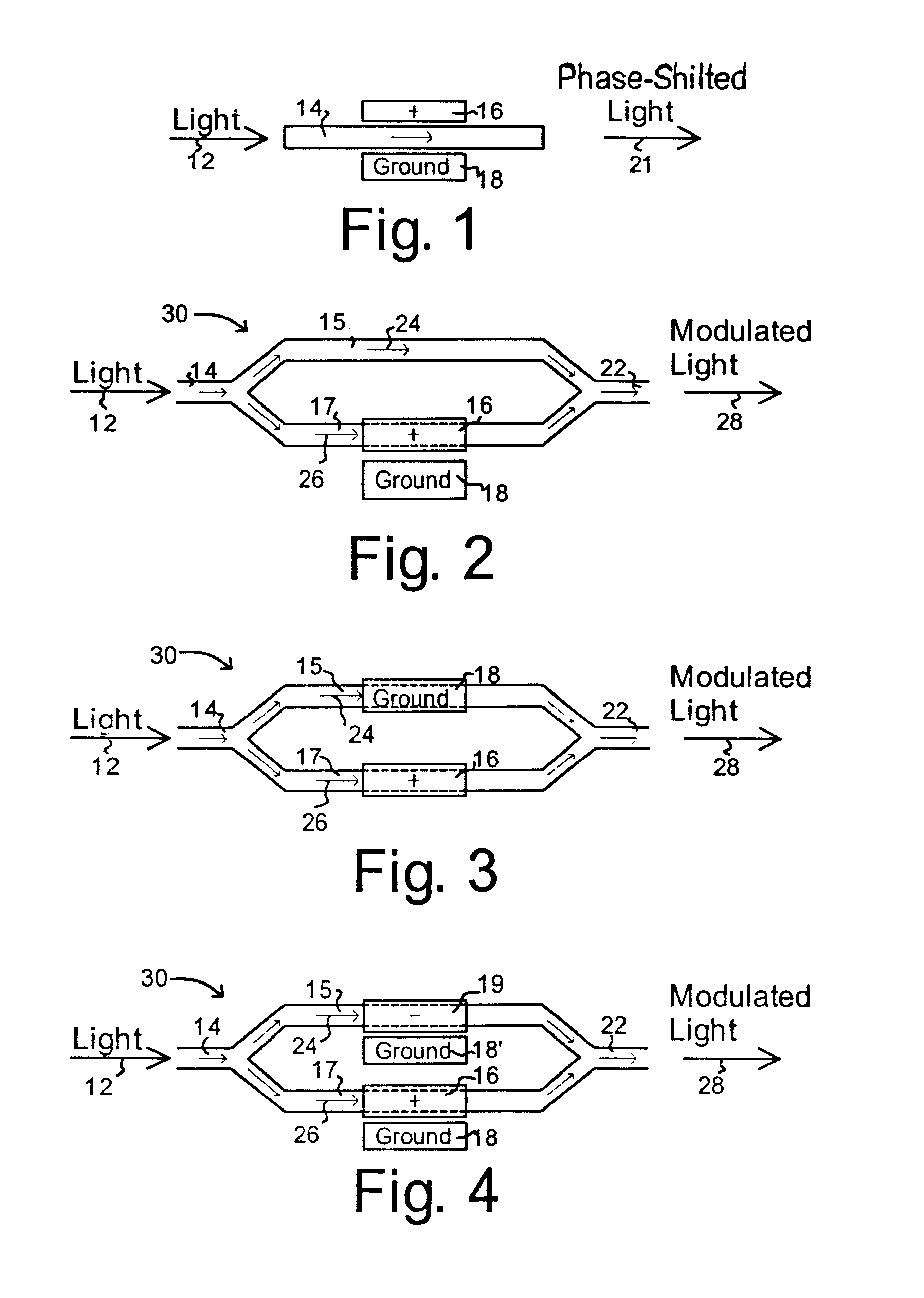
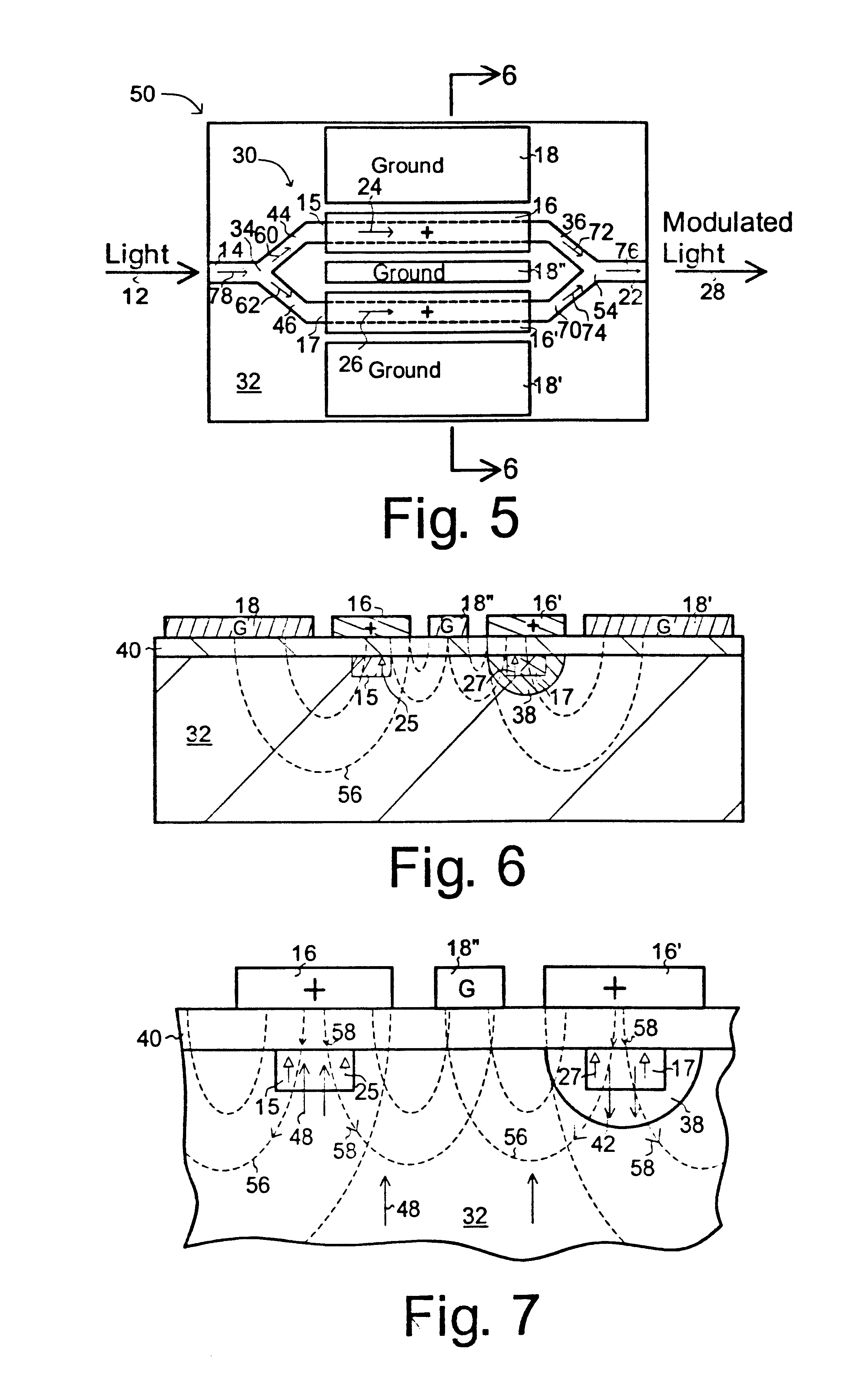
Generally two types of electro-optical modulators are currently in use, the phase modulator and the intensity modulator, which are shown generally in FIGS. 1 and 2. Both devices take advantage of the change in refractive index in a crystalline waveguide due to an applied voltage. In the optical, guided-wave phase modulator shown in FIG. 1, light 12 enters and travels along the waveguide 14 that has been placed between signal electrode 16 and ground electrode 18. An applied voltage at the signal electrode 16 introduces a change in the refractive index of the waveguide 14 which in turn alters the velocity of light passing through the waveguide causing a phase-shift in the emerging light 21 that is proportional to the applied voltage.

In FIG. 2, a guided-wave Mach-Zehnder (M-Z) interferometer intensity modulator 30 is used. Here light 12 enters waveguide 14 and is then split between two waveguide paths 15 and 17 and then joined again to leave via outlet guide 22. As with the phase-shift...


PUM

PropertyMeasurementUnit
thickaaaaaaaaaa
dielectric constantaaaaaaaaaa
reverse polarityaaaaaaaaaa

Abstract

An optical modulator has optical channels formed in a waveguide substrate in which two of the waveguide channel branches have reverse polarity relative to each other. In addition, the optical modulator has at least one of the following: 1) an electronic signal electrode and an electronic ground electrode are placed in proximity with opposite faces of the waveguide substrate, 2) a portion of said waveguide substrate is removed to afford a reduced electronic signal refractive index, and 3) the waveguide substrate has a fixing substrate attached to it with the refractive index of the fixing substrate lower than said refractive index of the waveguide substrate.

Description

1. Field of the InventionThis invention pertains to fiber optics and to a device that impresses information on an optical carrier to be transmitted by an optical fiber. More particularly it relates to electro-optical modulator devices using Mach-Zehnder-type modulators in which the first and second branches of the waveguide have reverse polarity and which further have one or more of the following characteristics: 1) the electronic signal driving voltage of the modulator is substantially lowered, 2) the electronic signal propagation velocity is close to the velocity of the optical carrier, 3) the electric field of the electronic signal is uniform and produces a net overlap of unity with the optical wave.2. Background of the InventionMach-Zehnder (M-Z) devices in which the first and second wave guide branches have reverse polarity was first demonstrated in U.S. Pat. No. 5,267,336 for electrode-less and lumped electrodes in push-pull configurations. To avoid the resistance-capacitance ...

Claims


Application Information

Patent Timeline
Patent Type & Authority Patents(United States)
IPC IPC(8): G02F1/01G02F1/225
CPCG02F1/225
Inventor SRIRAM, SRIRAM S.KINGSLEY, STUART A.
Owner SRICO
Why Eureka
Try Eureka