Functional verification of integrated circuit designs

a technology of integrated circuits and functional verification, applied in the field of electronic design of integrated circuits, can solve the problems of inability to meet the requirements of design and fabrication, the speed of verification may not be as important in the simulation environment, and the need for several weeks to redesign and complete fabrication

Inactive Publication Date: 2003-09-30
EVE
View PDF37 Cites 21 Cited by
  • Summary
  • Abstract
  • Description
  • Claims
  • Application Information

AI Technical Summary

Benefits of technology

If multiple blocks use less number of inputs than the number of address bits, the bits not formed using the input bit values can be used to select the functions. Assuming a RASD using an eight bit address and blocks using only five bits of inputs, the three bits can be used to select functions. Thus, the three bits can be used to identify eight functions, and the remaining five bits can be formed by the input data values such that the address of the location can be formed without much computational or storage requirements.
The above memory schemes can be combined, potentially even with other schemes, to increase the throughput performance and the size of the integrated circuit which can be supported. For example, the case when blocks use less number of inputs than the number of address bits (described in the preceding paragraph) can be combined with the case in which multiple outputs are stored in the location to retrieve output values of multiple blocks in a single memory access. In such a scenario, some bits of a memory address are formed by input data values and the other bits of the address identify a group of blocks. The individual bit positions represent the output values of individual blocks.
The present invention scales well to complex target designs because each block can have several inputs, and a block can be evaluated in a single memory access. That is, due to the ability to have blocks with several inputs, a complex target design can be divided into potentially large blocks, with each block being evaluated in a single memory access. Accordingly, complex target designs can be verified quickly.
The present invention is particularly suited for emulation environments as the output corresponding to a combination of input values can be generated quickly. The quickness may be achieved due to the pre-computation of the truth tables and accessing the values using random access memories.
The present invention is suited for simulation environments also as a verification system can be implemented in a cost-effective manner at the expense of lower throughput performance.
The present invention enables functional verification to be performed quickly as typical evaluation of blocks can be performed in a single memory access.

Problems solved by technology

Speed of verification may not be as important in simulation environments as cost of implementation.
In addition, it may require several weeks of time to redesign and complete fabrication again.
Such levels of delays may be unacceptable, particularly in the high-technology markets where short design cycles are generally important.
Such large times may also not be acceptable.
However, the size of the truth table can become unmanageable even with target designs of reasonable sizes as noted above with reference to FIG. 1.

Method used


Image

  • Functional verification of integrated circuit designs
  • Functional verification of integrated circuit designs
  • Functional verification of integrated circuit designs

Examples


verification chassis 520

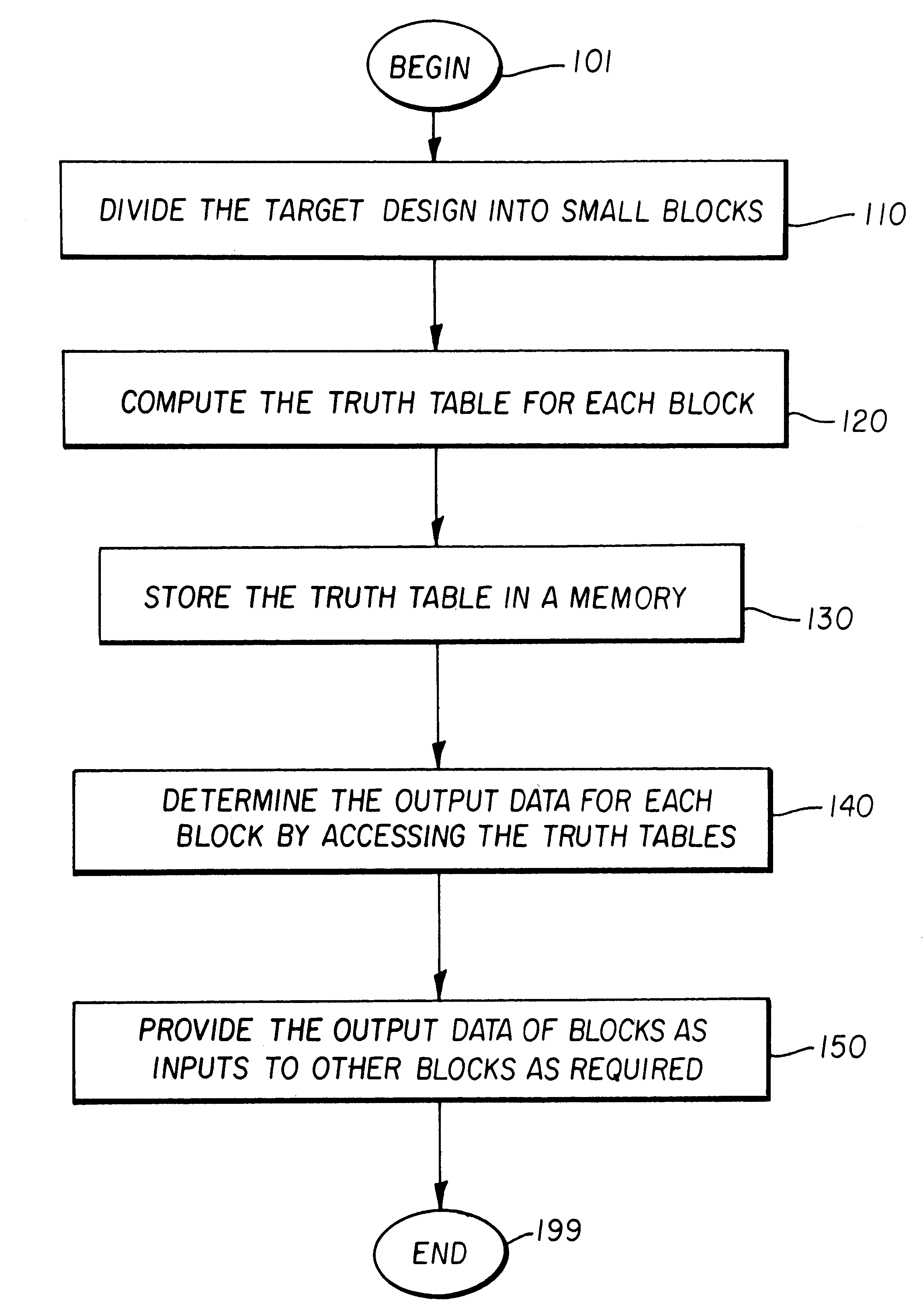
is configured according to the division performed by CLOG 510. Verification chassis 520 includes memory storage to store truth tables for the divided combinatorial blocks. The truth tables may be computed within Even though only one verification chassis 520 is shown in FIG. 5, it should be understood that multiple verification chassis may be employed to verify complex integrated circuits. Each verification chassis 520 may be viewed as including multiple verification units, with each verification unit evaluating one of more combinatorial logic blocks (as defined by CLOG 510). Communication scheme needs to be implemented among verification units to implement the dependencies in the target design. The communication typically needs to be intra-chassis and inter-chassis.

During the verification process, verification chassis 520 generates output data (primary or internal) corresponding to each state change in the target design. A state change may be caused either due to the logic implemen...

an example implementation

of verification chassis 520 is described first, followed by CLOG 510.

7. Verification Chassis 520

Continuing with reference to FIG. 5, an embodiment of verification chassis 520 can be implemented by modifying one of many commercially available chassis in the market place. Verification chassis 520 may include one or more boards (shown as 522-A through 522-Z), back-plane system 521, and power and cooling system 523. Verification boards 522-A through 522-Z are described with general reference to 522-X. Verification chassis 520 may contain multiple slots, with each verification board occupying a slot. Each verification board 520 may contain multiple combination logic output evaluation (CLOE) blocks shown as 523-A through 523-P. Each CLOE operates as a verification unit of one or more logic blocks.

Power and cooling system 523 provides the electrical power to the remaining components and maintains the temperature of all the components within any desired temperature in a known way. Back-plan...

an embodiment

of verification system 500 includes 16 slots in a single chassis 520. Verification boards (e.g., some of 552-A through 522-Z) can be plugged into one or more of these 16 slots. Chassis 520 may have back-plane 521 to inter-connect the 512 signals from each slot. Back-plane 510 may distribute signals from the target system, support workstation and from any other verification chassis to all the slots in this chassis. In addition the chassis may have three sets of cables (not shown in the drawings). One set would be to connect to target system 530 (for emulation environments). This cable set would carry all the primary signals to and from target system 530. The second set would be to connect to the support workstation, CLOG 510 (can be used for receiving input data and sending output data in simulation environments). This set would carry the control, initialization and support information. The last set would be to connect to other verification chassis. A cluster of verification chassis ...


PUM


Abstract

A functional verification system suited for verifying the function of cycle based integrated circuits (IC) design. The IC design is divided into a plurality of combinatorial blocks connecting sequential elements. Truth tables corresponding to the divided blocks are computed and stored in a memory. The output values of the IC design are determined by evaluating the blocks. The evaluation typically entails one memory access as the truth tables are pre-computed and stored in a memory storage. Accordingly the output values are computed quickly. The storage is implemented using random access memories and a XCON is designed to ensure the dependencies are preserved during the evaluations.

Description

1. Field of the InventionThe present invention relates to the electronic design of integrated circuits, and more specifically to a method and apparatus for the functional verification of a target integrated circuit design.2. Related ArtFunctional verification is one of the steps in the design of many integrated circuits. Functional verification generally refers to determining whether a design ("target design") representing an integrated circuit performs a function it is designed for. In a typical design process, a designer identifies the functions to be performed and designs a circuit using high-level languages (e.g., VHDL language well known in the relevant arts) to perform the identified functions. An example of a function may be to generate a predetermined output data corresponding to a given input data. Tools available in the industry are typically used to generate a lower-level design (e.g., at gate-level) from the design specified in a high-level language. The higher level lan...

Claims


Application Information

Patent Timeline
Patent Type & Authority Patents(United States)
IPC IPC(8): G06F17/50G01R31/28
CPCG06F17/5022G06F30/33
Inventor GANESAN, SUBBUPILLALAMARRI, SHYAM PRASAD
Owner EVE
Why Eureka
Try Eureka