
Phosphor thin film, preparation method, and EL panel

a technology of phosphor and thin film, applied in the field of phosphor thin film, preparation method, and el panel, can solve the problems of unsuitable color display, green and blue suffer from emission luminance, emission efficiency and color purity, and color el panel has not reached the commercial stag

Inactive Publication Date: 2003-12-02
IFIRE IP CORP
View PDF6 Cites 0 Cited by
  • Summary
  • Abstract
  • Description
  • Claims
  • Application Information

AI Technical Summary

Benefits of technology

Another object is to provide a phosphor thin film which enables to simplify the manufacture process of full-color EL panels, and offers the advantages of minimized variation of luminance, increased yields, and reduced manufacture cost, a method for preparing the same, and an EL panel.

Problems solved by technology

Thin-film EL displays using sulfide phosphor thin films are fully reliable and resistant to environment, but at present regarded unsuitable as color displays because EL phosphors required to emit light in the primaries of red, green and blue have poor characteristics.
These phosphor thin films capable of emitting light in the primaries of red, green and blue suffer from problems of emission luminance, emission efficiency and color purity.
Thus color EL panels have not reached the commercial stage.
These thiogallate base phosphors are satisfactory in color purity, but suffer from a low luminance and especially, difficulty to form a thin film of uniform composition because of the multi-component composition.
It is believed that thin films of quality are not obtainable because of poor crystallinity resulting from inconvenient composition control, formation of defects resulting from sulfur removal, and admittance of impurities; and these factors lead to a failure to increase the luminance.
In particular, thioaluminate base phosphors are quite difficult to control their composition.
This method, however, is quite difficult to control the sources of metals for the matrix material (SrIn.sub.2 S.sub.4) and the source of luminescent center substance (Eu) so as to accurately control the quantity of the luminescent center.
It is then understood that controlling the concentration of Eu to a precision within 5% is very difficult.
A film forming method capable of deriving a high luminance from one material fails to achieve a high luminance for a phosphor thin film of another color.
The manufacturing process becomes very complex, leading to an increased cost of panel manufacture.
Use of filters complicates the manufacture process and, still worse, brings about a lowering of luminance.
EL devices were prepared using the thin films, but they failed to produce the desired light emission.
If the substrate temperature is too high, the thin film of matrix material may have more asperities on its surface and contain pin holes therein, giving rise to the problem of current leakage on EL devices.
However, too thick a layer requires an increased drive voltage whereas too thin a layer results in a low emission efficiency.
If the pressure exceeds the range, the operation of the electron gun becomes unstable, and composition control becomes very difficult.
If the rotational speed of the substrate is too high, there may arise a problem of seal upon admission into the vacuum chamber.
If the rotational speed of the substrate is too low, compositional gradation may occur in the thickness direction within the chamber so that the characteristics of the light emitting layer may become poor.
This results in a high crystallinity thin film.

Method used


Image

  • Phosphor thin film, preparation method, and EL panel
  • Phosphor thin film, preparation method, and EL panel
  • Phosphor thin film, preparation method, and EL panel

Examples


example 1

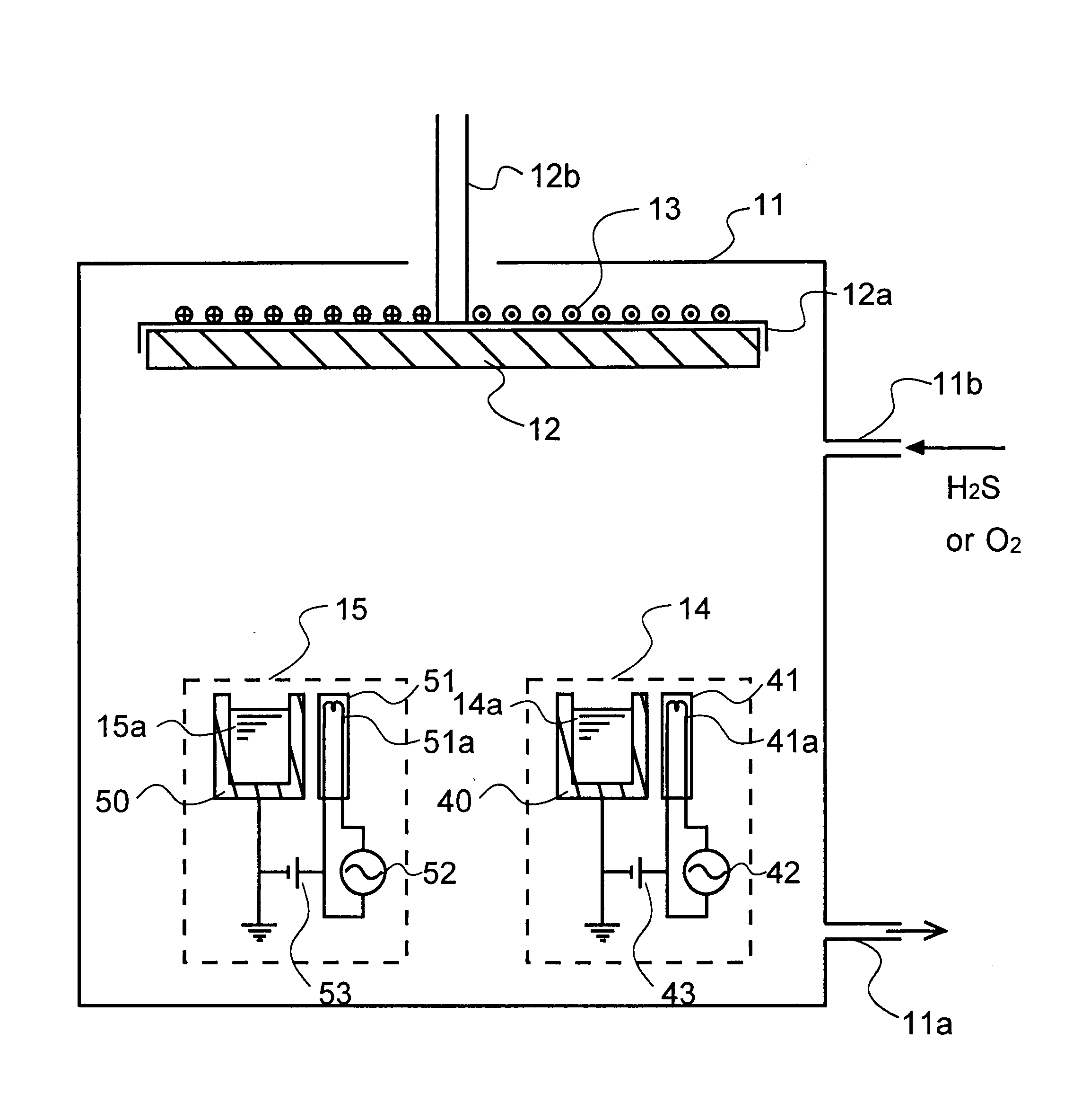
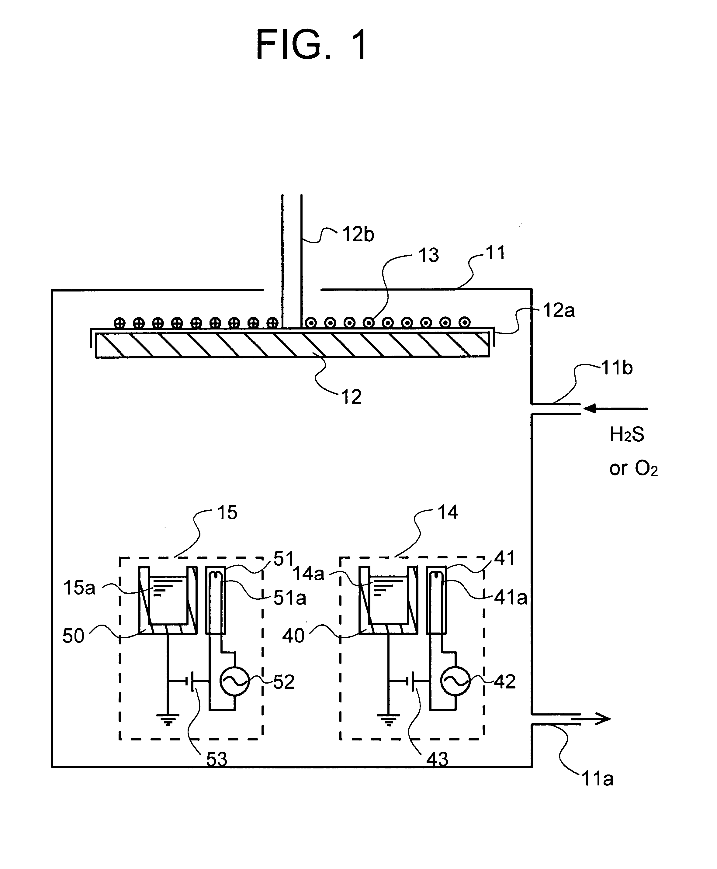
FIG. 1 illustrates an exemplary evaporation chamber which can be used in the manufacturing method of the invention. One electron gun and one resistive heating source (or cell) were used instead of two electron guns.

An EB source 15 containing EuS powder having 5 mol % of Ce.sub.2 S.sub.3 added and a cell source 14 containing Al.sub.2 S.sub.3 powder were placed in a vacuum chamber 11. The substances were simultaneously evaporated from the respective sources, and deposited on a rotating substrate heated at 400.degree. C., forming a EuAl.sub.2 S.sub.4 :Ce layer. The rates of evaporation from the respective sources were adjusted so as to give a deposition rate of 1 nm / sec for EuAl.sub.2 S.sub.4 and a molar ratio Eu:Al.sub.2 S.sub.3 of 1:1. During evaporation, H.sub.2 S gas was admitted at 20 SCCM. An insulating thin film was formed thereon, and the structure was annealed at 750.degree. C. for 10 minutes in air, yielding an oxysulfide phosphor thin film, EuAl.sub.2 O.sub.z S.sub.w :Ce.

The...

example 2

In Example 1, ytterbium (Yb) was used instead of Eu as the rare earth element, neodymium (Nd) was used instead of Ce, and Ga.sub.2 S.sub.3 was used instead of Al.sub.2 S.sub.3. Equivalent results were obtained, with emission of red light.

example 3

In Example 1, yttrium (Y) was used instead of Eu as the rare earth element, europium (Eu) was used instead of Ce, and In.sub.2 S.sub.3 was used instead of Al.sub.2 S.sub.3. Equivalent results were obtained, with emission of red light as well.


PUM

PropertyMeasurementUnit
molar ratioaaaaaaaaaa

Abstract

The invention aims to provide a phosphor thin film eliminating a need for filters, having a satisfactory color purity, suited for RGB in full-color EL displays, enabling to simplify the manufacture process of full-color EL panels, and offering the advantages of minimized variation of luminance, increased yields, and reduced manufacture cost, a method for preparing the same and an EL panel. Such objects are achieved by a phosphor thin film formed of a matrix material comprising an oxysulfide consisting of at least one compound selected from rare earth thioaluminates, rare earth thiogallates and rare earth thioindates, in which oxygen is incorporated, the matrix material further containing an element serving as a luminescent center, a method for preparing the same, and an EL panel using the same.

Description

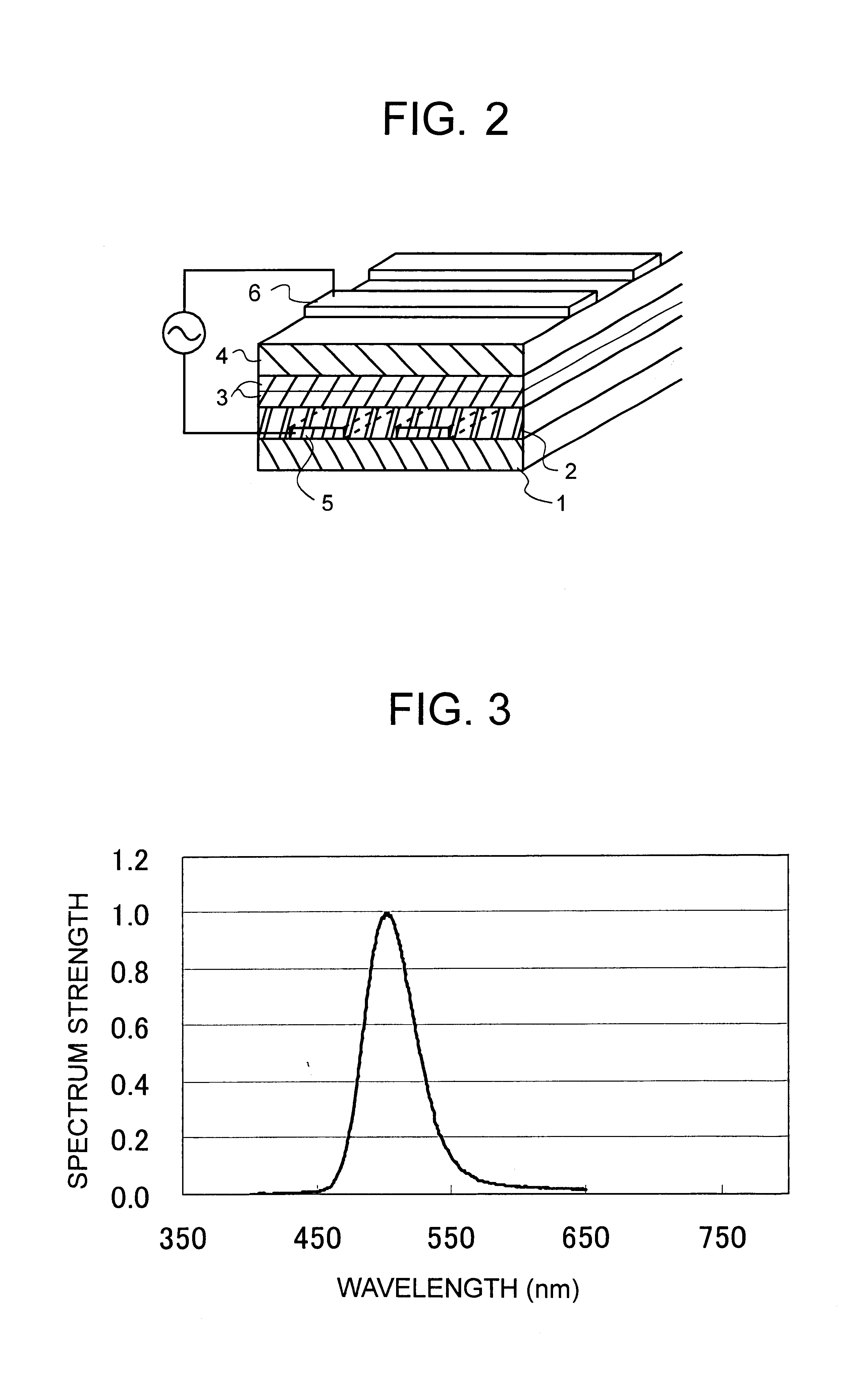
1. Technical FieldThis invention relates to an oxysulfide thin film having a light emitting function, and more particularly, to a phosphor thin film used as a light-emitting layer in inorganic EL devices and an EL panel using the same.2. Background ArtIn the recent years, active research works have been made on thin-film EL devices as small-size and large-size, lightweight flat displays. A monochromatic thin-film EL display using a phosphor thin film of manganese-doped zinc sulfide capable of emitting yellowish orange light has already become commercially practical as a dual insulated structure using thin-film insulating layers 2 and 4 as shown in FIG. 2. In FIG. 2, a predetermined pattern of lower electrodes 5 is formed on a substrate 1, and a first insulating layer 2 is formed on the lower electrodes 5. On the first insulating layer 2, a light-emitting layer 3 and a second insulating layer 4 are successively formed. On the second insulating layer 4, a predetermined pattern of uppe...

Claims


Application Information

Patent Timeline
Patent Type & Authority Patents(United States)
IPC IPC(8): C09K11/77H05B33/14C09K11/84
CPCC09K11/7771C09K11/7774C09K11/7792H05B33/14C09K11/7789Y10S428/917
Inventor YANO, YOSHIHIKOOIKE, TOMOYUKI
Owner IFIRE IP CORP
Learn More