Thin film inorganic light emitting diode

a light-emitting diode and thin film technology, applied in the direction of zinc sulfide, chemistry apparatus and processes, zinc sulfide, etc., can solve the problems of low fluorescent quantum yield, cumbersome and expensive vacuum-vapour deposition techniques, and low fluorescent quantum yield of tfel devices, so as to achieve easy and economical

Inactive Publication Date: 2004-03-16
AGFA GEVAERT AG
View PDF19 Cites 39 Cited by
  • Summary
  • Abstract
  • Description
  • Claims
  • Application Information

AI Technical Summary

Benefits of technology

It is the object of the present invention to provide an easy and economical method for the manufacturing of a Thin Film Inorganic Light Emitting Diode device capable of emitting light under the influence of direct current.
In a particularly preferred embodiment zinc sulfide is doped with manganese luminescent centres. Such a ZnS:Mn nanoparticle dispersion is prepared by a precipitation reaction performed by mixing appropriate aqueous solutions of the respective ions. Preferably, the precipitation reaction is performed according to the double jet principle whereby a first and a second solution are added simultaneously to a third solution under controlled conditions of flow rate. For instance, the first solution contains zinc ions, e.g. zinc acetate, and manganese ions, e.g manganese acetate ions. The second solution contains sulfide ions, e.g. sodium sulfide ions. These two solutions are added together to a third aqueous solution. In a preferred embodiment one of the solutions, preferably the third, contains a triazole or diazole compound. A preferred triazole compound is 5-methyl-1,2,4-triazolo-(1,5-a)-pyrimidine-7-ol. It is believed that the presence of such a compound enhances the incorporation of the Mn.sup.2+ dopant, and, as a result, the intensity of the luminescence.
Preferred binders are aqueous soluble polymers like polyvinyl alcohol (PVA) and polyvinyl pyrrolidone (PVP). Adding of these binders improves the stability of the dispersions.

Problems solved by technology

Crystallisation of initially amorphous samples, production of exciplexes with other materials, and often high chemical reactivity create serious problems in their application to stable EL systems.
Moreover, the layers are applied by using vacuum-vapour deposition techniques, which are often cumbersome and expensive.
The difficulties in purifiation procedures (and hence reproducability) and, mostly, a low fluorescent quantum yield, in addition to a complex structure and high sensitivity towards oxygen and moisture are severe drawbacks in their application to organic ELDs.
TFEL devices are used for high information content matrix displays and can only be produced on glass substrates, due to the high processing temperature needed.
The thick layer causes a slow luminance-voltage response, making PEL devices unsuitable for display applications.
General drawbacks of these PELDs are price (large amounts of products needed (about 150 g phosphor per square meter), the expensive BaTiO.sub.3 layer, the high driving voltages (around 110 V) and their inherent instability.
General drawbacks of this system are the slow and expensive production process and the necessity of complete protection against ambient humidity.
This results in a current drop which is associated with the onset of light emission.
Major drawbacks of this system are the irreproducability of the forming process and the necessity of complete encapsulation against moisture.
No commercial devices based on this principle are on the market today.
However, the use of Cd- or Se-compounds can not be recommended due to environmental problems that can be expected.
The drawback of their system lies in the fact that the synthesis of the ZnS:Cu particles is quite cumbersome and results in low yields.
Green electroluminescence could be observed in both bias directions at 5 V. The drawback of the fabrication of this device is the low concentrations of the ZnS:Cu dispersion that can be obtained (ca 10.sup.-3 M).
Also a drawback could be the solvent based spincoating dispersion.

Method used


Image

  • Thin film inorganic light emitting diode
  • Thin film inorganic light emitting diode
  • Thin film inorganic light emitting diode

Examples


example 1

Preparation of a ZnS:Mn Dispersion

The following solutions were prepared:

To solution 3, stirred at 1500 rpm at 80.degree. C., solutions 1 and 2, both held at room temperature, were added simultaneously at a flow rate of 500 ml / min. This results in a predispersion comprising ZnS:Mn--particles.

To 1000 ml of this predispersion, 1000 ml of a 2% Na-polyphosphate solution in water was added and this dispersion was diafiltrated through a Fresenius F60 cartridge. The dispersion was concentrated to 1000 ml and washed at this level by using 6000 ml of a 2% solution of Na-polyphosphate in water.

After the washing, this dispersion was concentrated by means of a diafiltration set-up to a concentration of about 35 g ZnS / l. Subsequently, 1 ml of a 12.5% solution of Saponine Quillaya (Schmittmann) in water / ethanol (80 / 20) solution per 20 ml dispersion was added. This is the final ZnS:Mn dispersion.

The dispersion was analysed for its particle size distribution with the Disc Centrifuge Photosedimentome...

example 2

Preparation of a ZnS:Cu Dispersion

The following solutions were prepared:

To solution 6, stirred at 1500 rpm at 80.degree. C., solutions 4 and 5, both held at room temperature, were added simultaneously at a flow rate of 500 ml / min. This results in a predispersion comprising ZnS:Cu--particles.

To 1000 ml of this predispersion, 1000 ml of a 2% Na-polyphosphate solution in water was added and this dispersion was diafiltrated through a Fresenius F60 cartridge. The dispersion was concentrated to 1000 ml and washed at this level by using 6000 ml of a 2% solution of Na-polyphosphate in water.

After the washing, this dispersion was concentrated by means of a diafiltration set-up to a concentration of about 35 g ZnS / l. Subsequently, 1 ml of a 12.5% solution of Saponine Quillaya (Schmittmann) in water / ethanol (80 / 20) solution per 20 ml dispersion was added. This is the final ZnS:Cu dispersion.

The dispersion was analysed for its particle size distribution with the Disc Centrifuge Photosedimentome...


PUM

PropertyMeasurementUnit
thickaaaaaaaaaa
thickaaaaaaaaaa
thickaaaaaaaaaa

Abstract

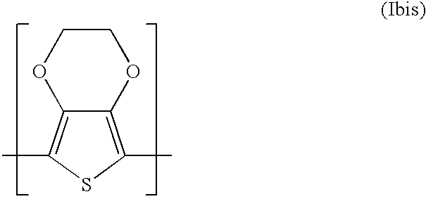
A method for the manufacturing of a Thin Film Inorganic Light Emitting Diode is disclosed. The device contains in one single layer or in a double layer a dispersion of zinc sulfide doped with a luminescent centre, and a water-compatible p-type semiconductive polymer, preferably a polythiophene / polymeric polyanion complex.

Description

The present invention relates to a particular type of a Thin Film Inorganic Light Emitting Diode.At present several thin film electroluminescent devices (ELDs) exist or are still in development. They are all characterized by one (or more) electroluminescent active layer(s) sandwiched between two electrodes. Optionally a dielectric layer may also occur. The substrate can be plastic or glass.The thin film ELDs can be subdivided into the organic and the inorganic based ELDs. The organic based thin film ELDs.sup.(1) are further subdivided into Organic molecular or Oligomeric Light Emitting Diodes (OLEDs) and Polymer Light Emitting Diodes (PLEDs). The inorganic ELDs on the other hand can be further subdivided into the High Voltage Alternating Current (HV-AC) ELDs and the Low Voltage Direct Current (LV-DC) ELDs. Amongst the HV-AC ELDs, one can distinguish Thin Film ElectroLuminescent Devices (TFEL devices or TFELDs) and Powder ELDs (PEL Devices or PELDs). Amongst LV-DC ELDs one can distin...

Claims


Application Information

Patent Timeline
Patent Type & Authority Patents(United States)
IPC IPC(8): C01G9/00C01G9/08C09K11/06C09C1/04H01L33/00H01L51/50H01L51/52H01L33/08H01L33/18H01L33/28H01L33/50
CPCB82Y30/00C01G9/08C09C1/04C09K11/06C01P2002/04C01P2002/52C01P2002/54C01P2002/84C01P2004/03C01P2004/04C01P2004/51C01P2004/64C01P2004/84C01P2006/40C01P2006/60H01L33/08H01L33/18H01L33/28H01L33/502H01L51/5203H10K50/805
Inventor ANDRIESSEN, HIERONYMUS
Owner AGFA GEVAERT AG
Why Eureka
Try Eureka