Double diffused MOS transistor and method for manufacturing same

a technology of mos transistor and mos, which is applied in the direction of transistors, semiconductor devices, electrical equipment, etc., can solve the problems of increasing the need for mounting small-sized, highly integrated semiconductor devices that consume a small amount of power on a semiconductor chip, and the limited high-energy ion implantation techniques

Inactive Publication Date: 2004-08-10
SAMSUNG ELECTRONICS CO LTD
View PDF2 Cites 31 Cited by
  • Summary
  • Abstract
  • Description
  • Claims
  • Application Information

AI Technical Summary

Benefits of technology

In an exemplary embodiment, the present invention is directed to a method of forming a semiconductor device, where a first layer may be formed on a semiconductor substrate, and one or more isolation trenches may be formed and filled with an isolation layer. A second layer may be formed on the first layer and semiconductor substrate, and a plurality of drain trenches may be formed therein. A pair of plug-type drains may be formed in the trenches, to be separated from the isolation layer by a dielectric spacer. Gates and source areas may be formed on a resultant structure containing the plug-type drains. Accordingly, current may be increased with a reduction in drain-source on resistance, and an area of the isolation layer can be efficiently reduced, as compared to an existing isolation layer, potentially resulting in a reduction in chip area.

Problems solved by technology

Additionally where high-energy ion implantation is used to reduce Rdson, since high-dose doping may be difficult, high-energy ion implantation techniques may be limited when reducing Rdson, since these techniques cannot avoid the diffusion of impurity ions in a vertical direction.
Thus, high-energy ion implantation techniques may be disadvantageous to the scaling of the semiconductor device.
However, the need for mounting small-sized, highly-integrated semiconductor devices that consume a small amount of power on a semiconductor chip continues to increase.

Method used


Image

  • Double diffused MOS transistor and method for manufacturing same
  • Double diffused MOS transistor and method for manufacturing same
  • Double diffused MOS transistor and method for manufacturing same

Examples


Embodiment Construction

Hereinafter, exemplary embodiments of the present invention will be described in detail with reference to the attached drawings. However, the exemplary embodiments of the present invention can be modified into various other forms, and the scope of the present invention must not be interpreted as being restricted to the exemplary embodiments. The exemplary embodiments are provided to more completely explain the present invention to those skilled in the art. In drawings, the thicknesses of layers or regions are exaggerated for clarity. Like reference numerals in the drawings denote the same members. Also, when it is written that a layer is formed "on" another layer or a substrate, the layer can be formed directly on the other layer or the substrate, or other layers can intervene therebetween.

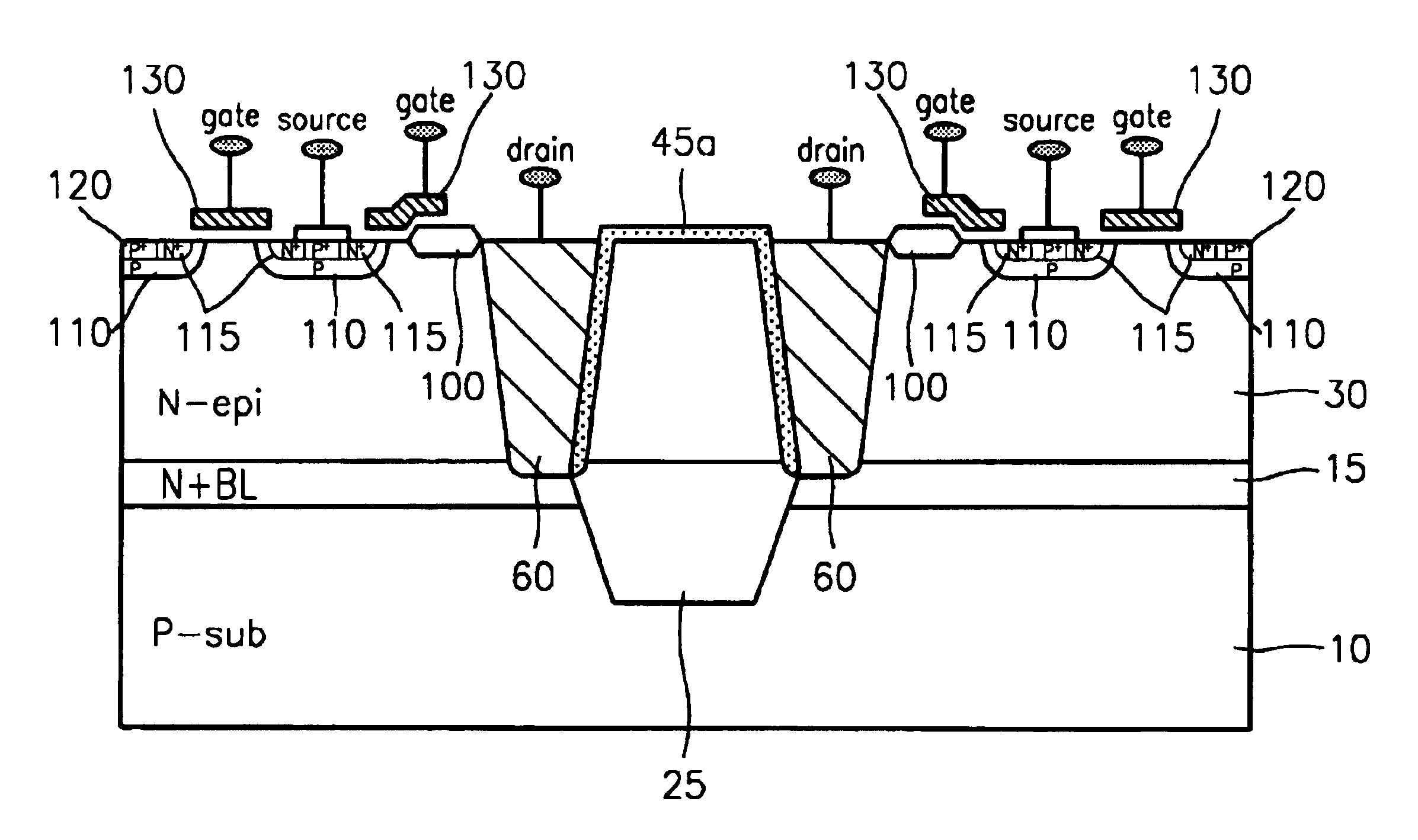
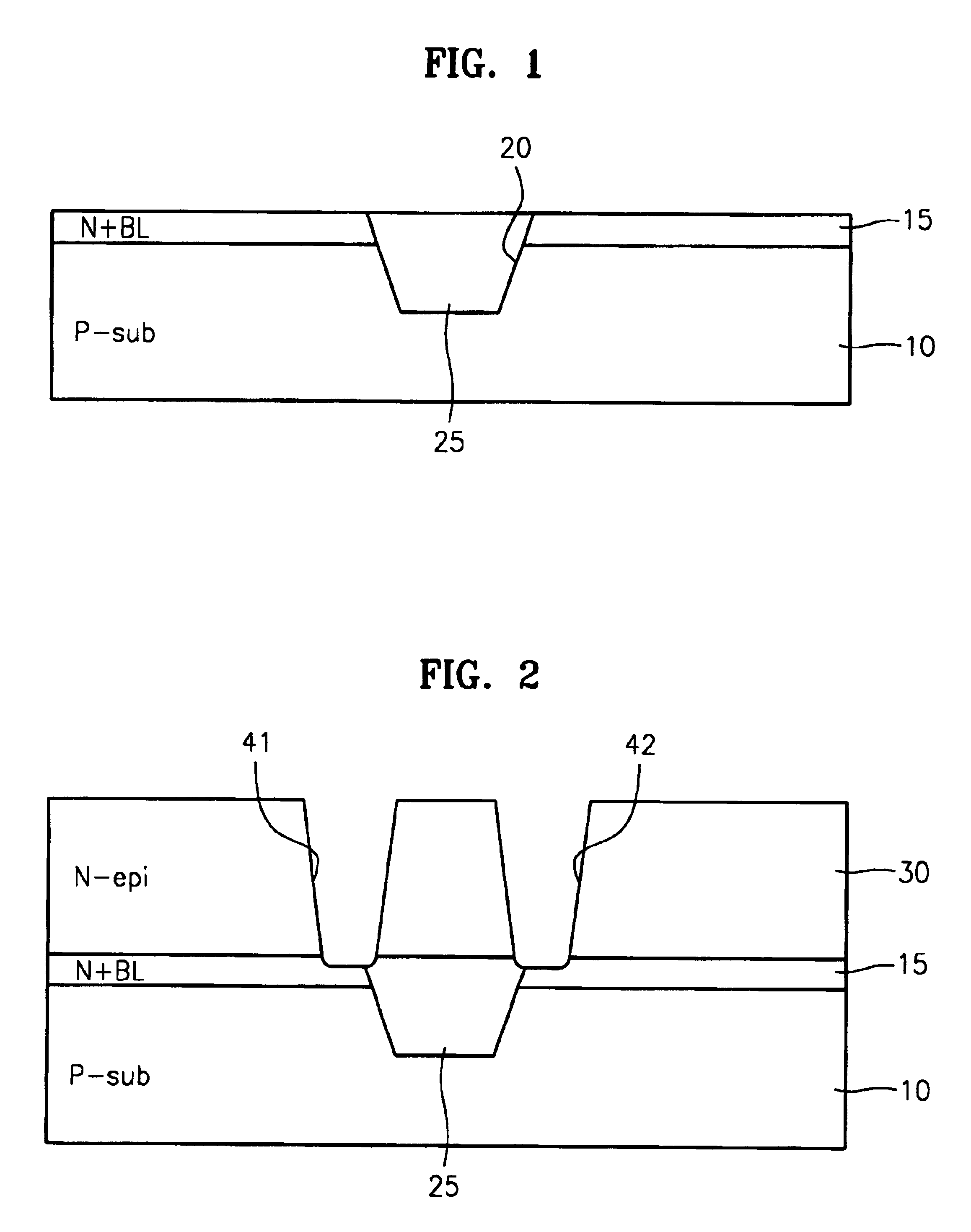
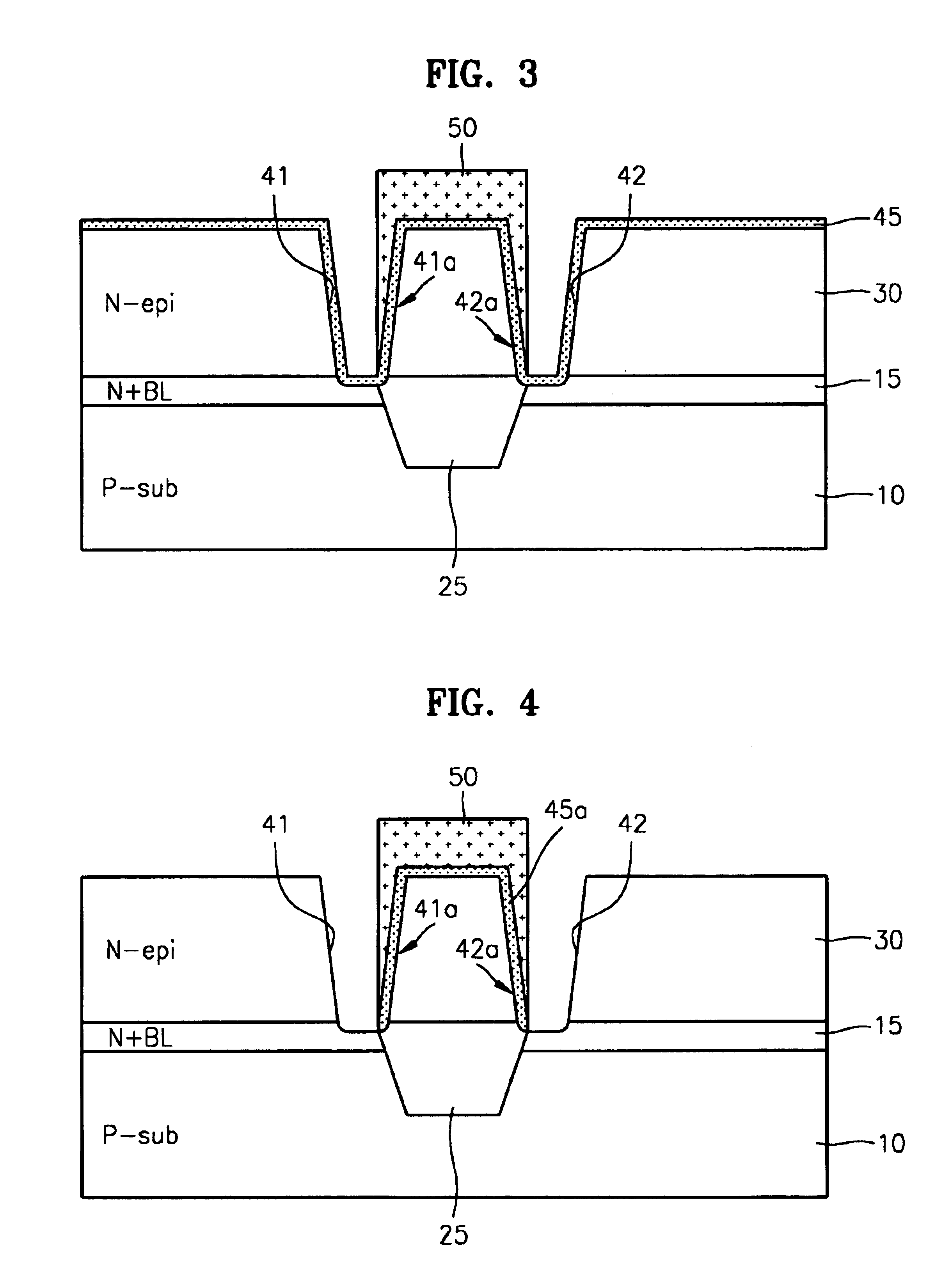
FIGS. 1 through 6 are cross-sectional views describing a method of manufacturing a VDMOS transistor according to an exemplary embodiment of the present invention. First, referring to FIG. 1, a sem...


PUM


Abstract

A method of manufacturing a semiconductor device, such as a double-diffused metal oxide semiconductor (DMOS) transistor, where a first layer may be formed on a semiconductor substrate, with isolation trenches formed in the first layer and semiconductor substrate, and with the trenches being filled with an isolation layer. A second layer may be formed on the first layer and semiconductor substrate, and a plurality of drain trenches may be formed therein. A pair of plug-type drains may be formed in the trenches, to be separated from the isolation layer by a dielectric spacer. Gates and source areas may be formed on a resultant structure containing the plug-type drains. Accordingly, current may be increased with a reduction in drain-source on resistance, and an area of the isolation layer can be reduced, as compared to an existing isolation layer, potentially resulting in a reduction in chip area.

Description

CROSS-REFERENCE TO RELATED CASESThis application claims the priority of Korean Patent Application No. 2002-0043697, filed Jul. 24, 2002, in the Korean Intellectual Property Office, the disclosure of which is incorporated herein in its entirety by reference.1. Field of the InventionThe present invention relates to a power device and a method for manufacturing the same.2. Description of the Related ArtDouble-diffused metal oxide semiconductor (DMOS) transistors, which are MOS-type transistors driven by voltage and which may bear high current, have begun attracting greater attention. DMOS transistors integrated with bipolar-type integrated circuits may be classified as lateral DMOS (LDMOS) transistors, or vertical DMOS (VDMOS) transistors, depending on the direction of current flowing therein. In particular, for DMOS transistors operating at a high voltage, it is advantageous that the DMOS transistors be VDMOS transistors because VDMOS transistors occupy smaller area on a substrate tha...

Claims


Application Information

Patent Timeline
Patent Type & Authority Patents(United States)
IPC IPC(8): H01L21/70H01L29/78H01L29/66H01L21/8234H01L29/02H01L29/417H01L29/40H01L29/06H01L21/336H01L21/76H01L27/04H01L27/08H01L27/088
CPCH01L21/823487H01L29/7809H01L29/0653H01L29/41766H01L29/78
Inventor SHIN, HWA-SOOKLEE, SOO-CHEOL
Owner SAMSUNG ELECTRONICS CO LTD
Why Eureka
Try Eureka