

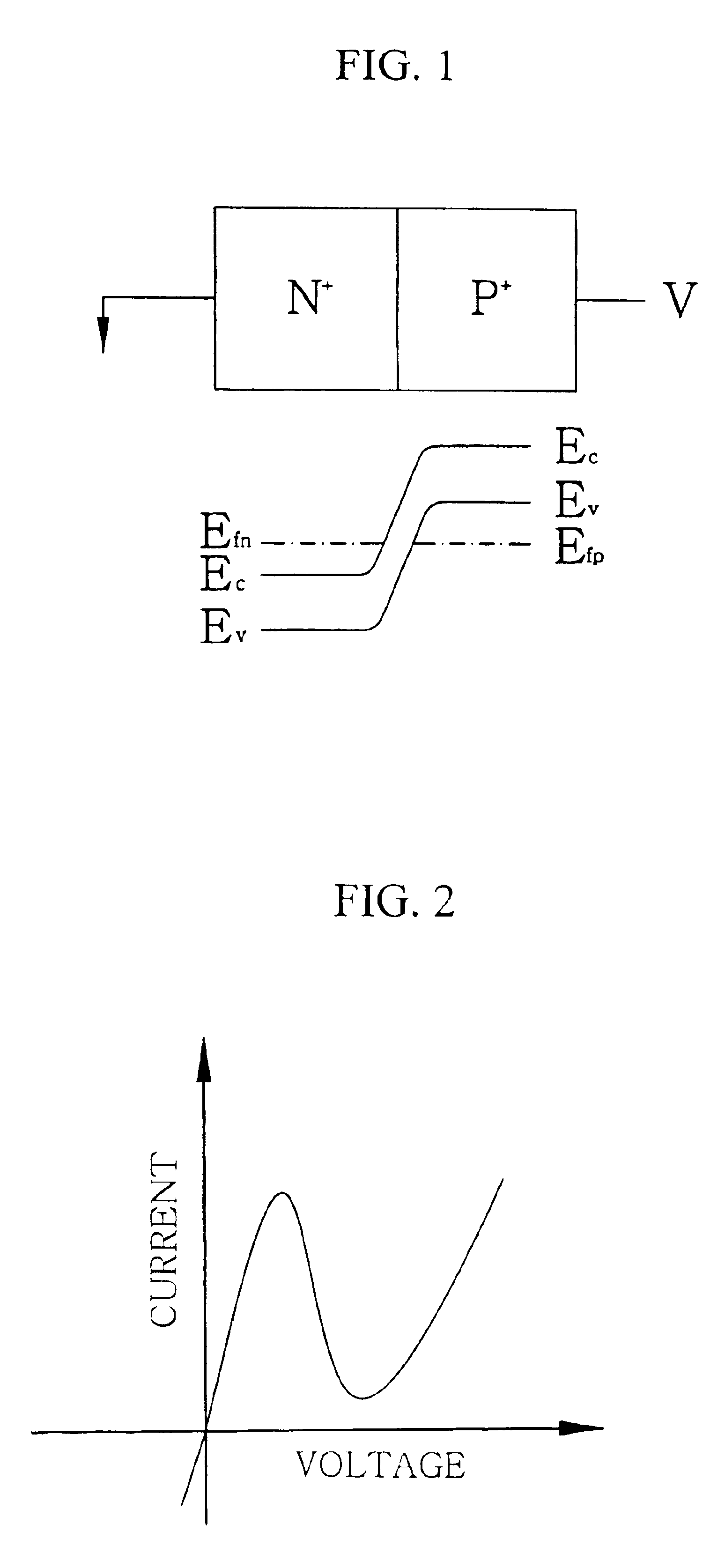
Method for fabricating semiconductor device with negative differential conductance or transconductance
a technology of differential conductance or transconductance, which is applied in the direction of semiconductor devices, electrical devices, nanotechnology, etc., can solve the problems of device problem in view of active operation, device operation limit, and process complexity
- Summary
- Abstract
- Description
- Claims
- Application Information
AI Technical Summary
Benefits of technology
Problems solved by technology
Method used
Image

Examples
first embodiment
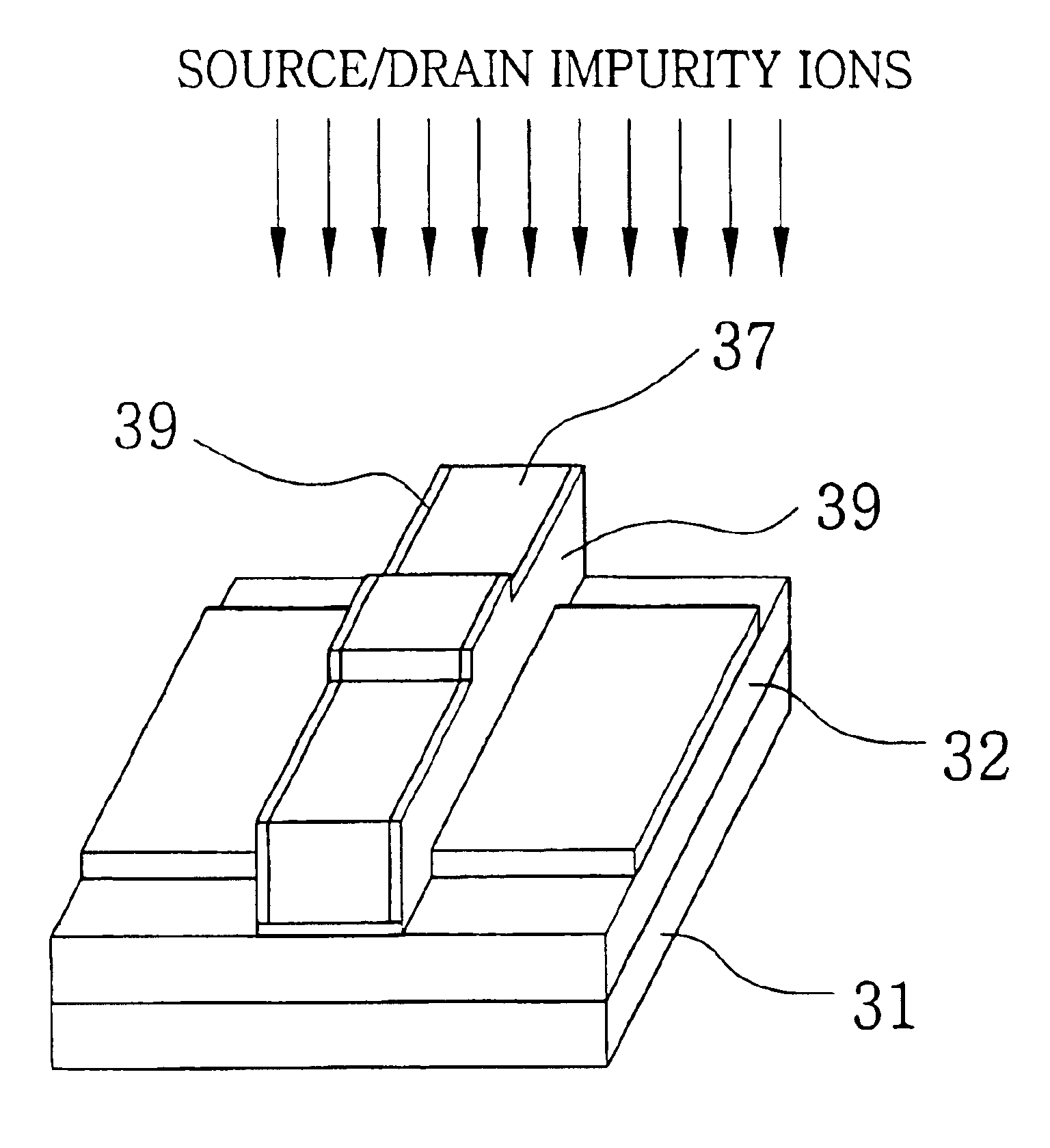
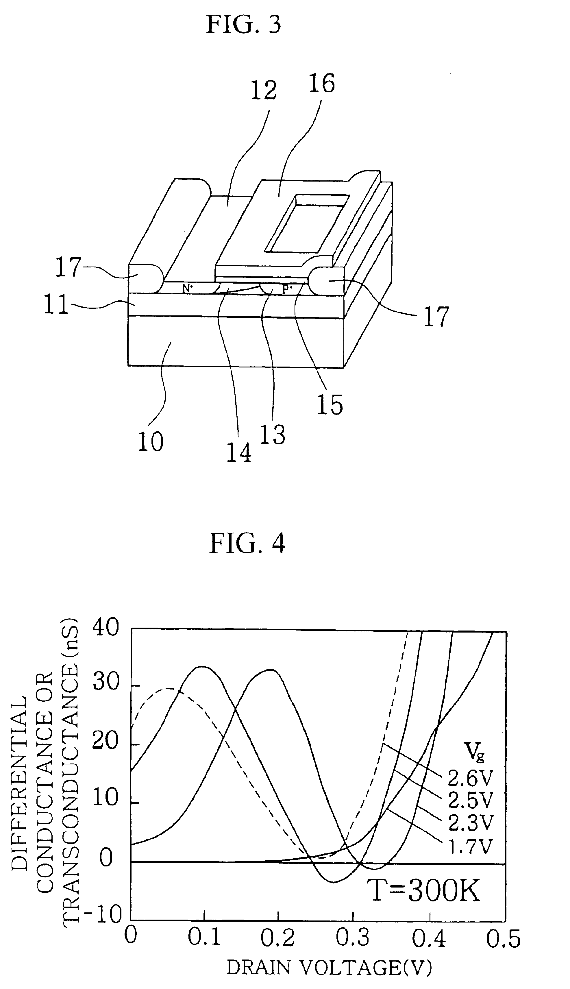
FIGS. 5a to 5h are perspective views showing sequential processes of fabricating a semiconductor device with negative differential conductance or transconductance according to the present invention. As shown in FIG. 5a, an SOI (Silicon on Insulator) substrate consisting sequentially of a silicon support 31, a buried oxide film 32 and a single crystal silicon layer 33 is first prepared.
The single crystal silicon layer 33 is then etched off with an E-beam lithography method or a fine patterning technique using sidewalls so that a source region 33a, a channel region 33b with a fine line width, and a drain region 33c are formed (see FIG. 5b).
After a sacrificial oxide film 34 having the thickness of about 50 .ANG. is formed on the entire surface including the source, channel and drain regions 33a to 33c and impurity ions are implanted on the entire surface with their density being higher than the effective density of states at which electrons or holes can exist so that the channel region...
embodiment 2
In the first embodiment of the present invention, after the impurity ions are first implanted into the channel region 33b and the gate 37 having a fine line width are formed, the impurity ions are then implanted into the source / drain regions 33a, 33c. In this embodiment, the impurity ions implanted into the source / drain regions 33a, 33c may be overly and laterally diffused in the thermal process for activation of the impurity ions, inviting a problem that the impurity ions in the source / drain regions may encroach the channel region 33b.
second embodiment
In order to solve this problem, the order of implanting the impurity ions into the channel and source / drain regions is changed in the present invention.
FIGS. 7a to 7f are perspective views showing sequential processes of fabricating a semiconductor device with negative differential conductance or transconductance according to the second embodiment of the present invention.
After performing the process of FIG. 5c (that is, after forming the sacrificial oxide film 34), impurity ions are implanted into the entire surface with their density being higher than the effective density of states at which electrons or holes can exist so that the source / drain regions 33a, 33c can be doped with the impurity ions, as shown in FIG. 7a.
PUM
 Abstract
Description
Claims
Application Information