

Integrated chip package structure using ceramic substrate and method of manufacturing the same
a technology of integrated chips and ceramic substrates, which is applied in the direction of electrical equipment, semiconductor devices, semiconductor/solid-state device details, etc., can solve the problems of increasing reducing the distance of the signal transmission path, and increasing the delay and attenuation of the signal
- Summary
- Abstract
- Description
- Claims
- Application Information
AI Technical Summary
Benefits of technology
Problems solved by technology
Method used
Image

Examples
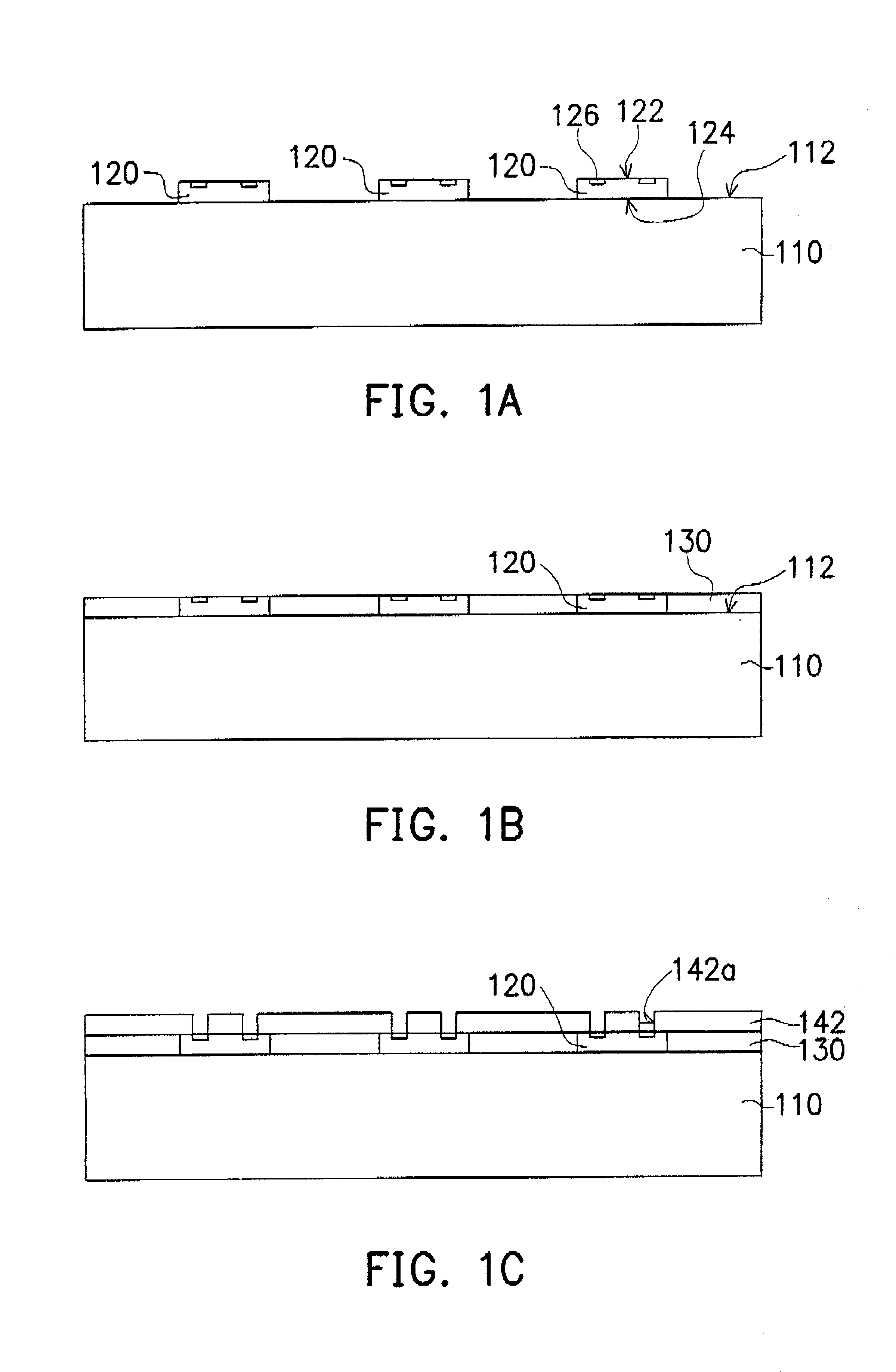
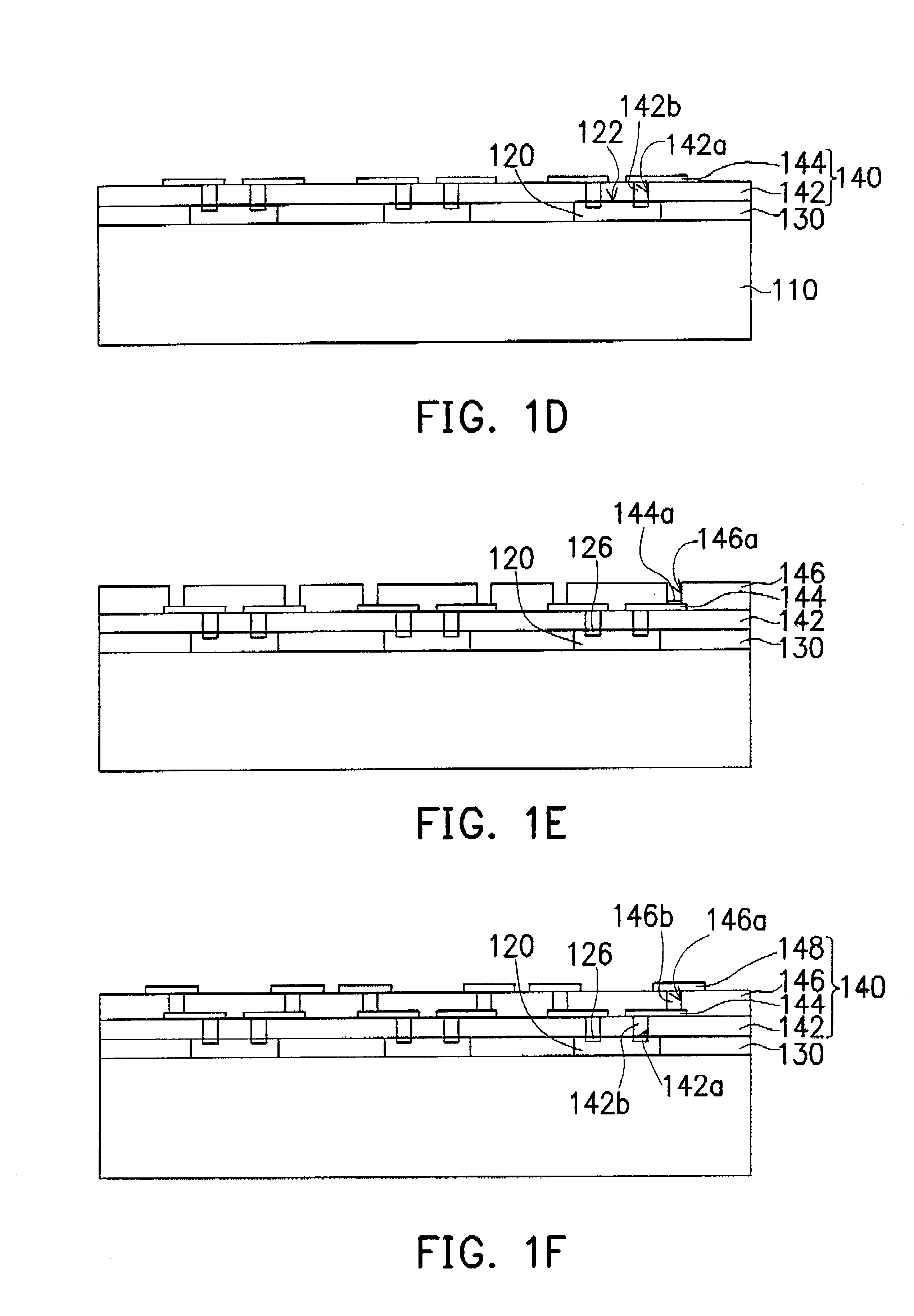
first embodiment
According to the above, the present invention is a chip package structure with a ceramic substrate and a plurality of dies on it. The external circuitry of the thin-film circuit layer allows the metal pads of the die to fan out. By forming bonding pads corresponding to the metal pads of the dies such as solders balls, bumps, or pins as the signal input terminals, the distance of the signal path is effectively decreased. As a result, signal delay and attenuation are reduced to increase performance of the die.
Ceramic material possesses advantageous properties such as high structural rigidity, high anti-corrosive properties, high density, and high thermal conductivity. Coefficient of thermal expansion (CTE) of aluminum oxide ceramic material is comparable to that of iron-cobalt-nickel alloy. The present invention specifically applies the use of ceramic material due to its high structural rigidity, high anti-corrosive properties, high density, and high thermal conductivity, which means ...
second embodiment
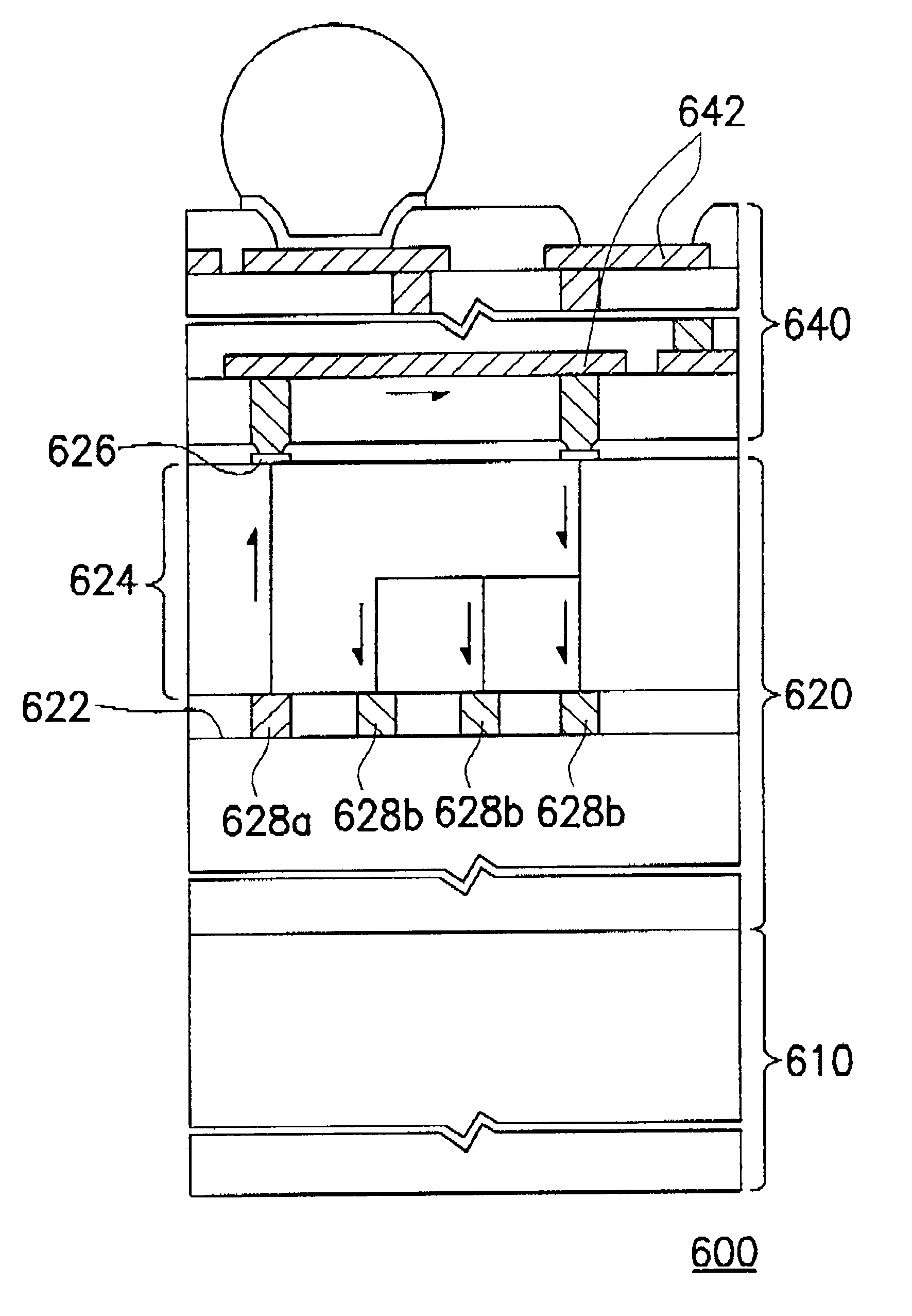
the present invention is a ceramic substrate with a plurality of inwardly protruded areas for inlaying dies by adhering the backside of the dies to the bottom of the inwardly protruded areas and exposing the active surface of the dies. A thin-film circuit layer is formed on top of the dies and the ceramic substrate to fan out the metal pads of the dies by using the external circuitry of the thin-film circuit layer. Due to the inlay of the dies in the ceramic substrate, thinning of the thickness of the chip package structure is effectively achieved and the surface of the ceramic substrate provides enough planarity and support for the formation of the thin-film circuit layer.
The third embodiment of the present invention differs from the second embodiment of the present invention by using an integrated ceramic substrate with at least one ceramic layer and one heat conducting layer. FIGS. 3A to 3C are schematic diagrams of the sectional view of the third embodiment illustrating the fabr...
third embodiment
the present invention is an integrated ceramic substrate with a ceramic layer with a plurality of openings and a heat conducting layer. The openings in the ceramic layer will form inwardly protruded areas on the integrated ceramic substrate. Backside of the die adheres to the bottom of the inwardly protruded areas so the dies are inlayed in the inwardly protruded areas exposing the active surface of the dies. This integrated ceramic substrate can efficiently dissipate heat from the dies to the outside because the bottom of the inwardly protruded area is the surface of the heat conducting material. The surface of the ceramic substrate provides enough planarity and support for the formation of the thin-film circuit layer.
The fourth embodiment of the present invention is slightly different from the first three embodiments. FIGS. 4A to 4E are schematic diagrams of the sectional view of the fourth embodiment illustrating the fabrication of the structure.
Please refer to FIG. 4A, a ceramic...
PUM
 Abstract
Description
Claims
Application Information