Run-to-run control method for proportional-integral-derivative (PID) controller tuning for rapid thermal processing (RTP)

a technology of proportional integration and controller tuning, applied in the direction of electric controllers, semiconductor/solid-state device testing/measurement, instruments, etc., can solve the problems of engendering nonoptimal control of critical processing parameters, many of the processing tools currently commercially available suffer certain deficiencies, and many tools lack advanced process data monitoring capabilities

Inactive Publication Date: 2004-11-16
ADVANCED MICRO DEVICES INC
View PDF7 Cites 12 Cited by
  • Summary
  • Abstract
  • Description
  • Claims
  • Application Information

AI Technical Summary

Problems solved by technology

However, despite the advances made in this area, many of the processing tools that are currently commercially available suffer certain deficiencies.
In particular, such tools often lack advanced process data monitoring capabilities, such as the ability to provide historical parametric data in a user-friendly format, as well as event logging, real-time graphical display of both current processing parameters and the processing parameters of the entire run, and remote, i.e., local site and worldwide, monitoring.
These deficiencies can engender nonoptimal control of critical processing parameters, such as throughput accuracy, stability and repeatability, processing temperatures, mechanical tool parameters, and the like.
The rapid thermal processing (RTP) performance typically degrades with consecutive process runs, in part due to drift in the respective settings of the rapid thermal processing (RTP) tool and / or the rapid thermal processing (RTP) sensors.
This may cause differences in wafer processing between successive runs or batches or lots of wafers, leading to decreased satisfactory wafer throughput, decreased reliability, decreased precision and decreased accuracy in the semiconductor manufacturing process.
However, traditional statistical process control (SPC) techniques are often inadequate to control precisely process parameters related to rapid thermal processing (RTP) in semiconductor and microelectronic device manufacturing so as to optimize device performance and yield.
Furthermore, blindly minimizing non-adaptive processing spreads about target values may not increase processing yield and throughput.
Traditional control techniques are frequently ineffective in reducing off-target processing and in improving sort yields.
When one or more of the processing steps are producing resulting wafers that wafer electrical test (WET) measurements indicate are unacceptable, causing the resulting wafers to be scrapped, this misprocessing goes undetected and uncorrected for quite a while, often for weeks, leading to many scrapped wafers, much wasted material and decreased overall throughput.

Method used


Image

  • Run-to-run control method for proportional-integral-derivative (PID) controller tuning for rapid thermal processing (RTP)
  • Run-to-run control method for proportional-integral-derivative (PID) controller tuning for rapid thermal processing (RTP)
  • Run-to-run control method for proportional-integral-derivative (PID) controller tuning for rapid thermal processing (RTP)

Examples


Embodiment Construction

Illustrative embodiments of the invention are described below. In the interest of clarity, not all features of an actual implementation are described in this specification. It will of course be appreciated that in the development of any such actual embodiment, numerous implementation-specific decisions must be made to achieve the developers' specific goals, such as compliance with system-related and business-related constraints, which will vary from one implementation to another. Moreover, it will be appreciated that such a development effort might be complex and time-consuming, but would nevertheless be a routine undertaking for those of ordinary skill in the art having the benefit of this disclosure.

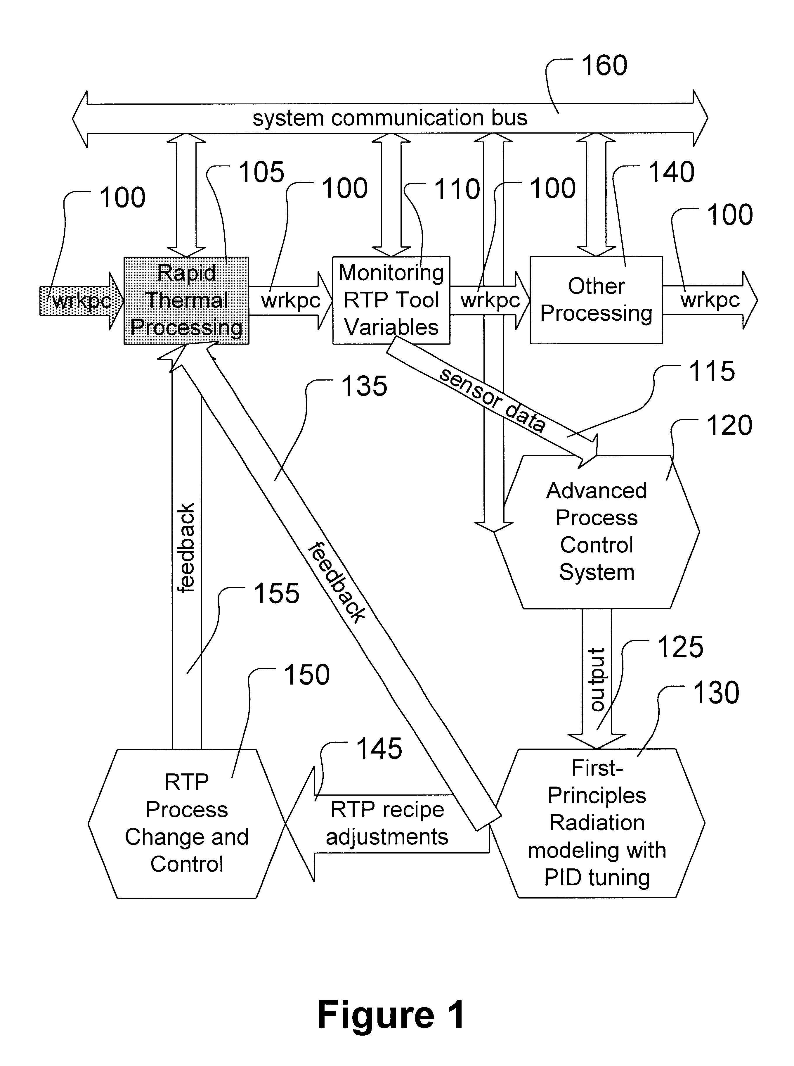
Illustrative embodiments of a method according to the present invention are shown in FIGS. 1-23. As shown in FIG. 1, a workpiece 100, such as a semiconducting substrate or wafer, having zero, one or more process layers and / or semiconductor devices, such as a metal-oxide-semiconductor (...


PUM


Abstract

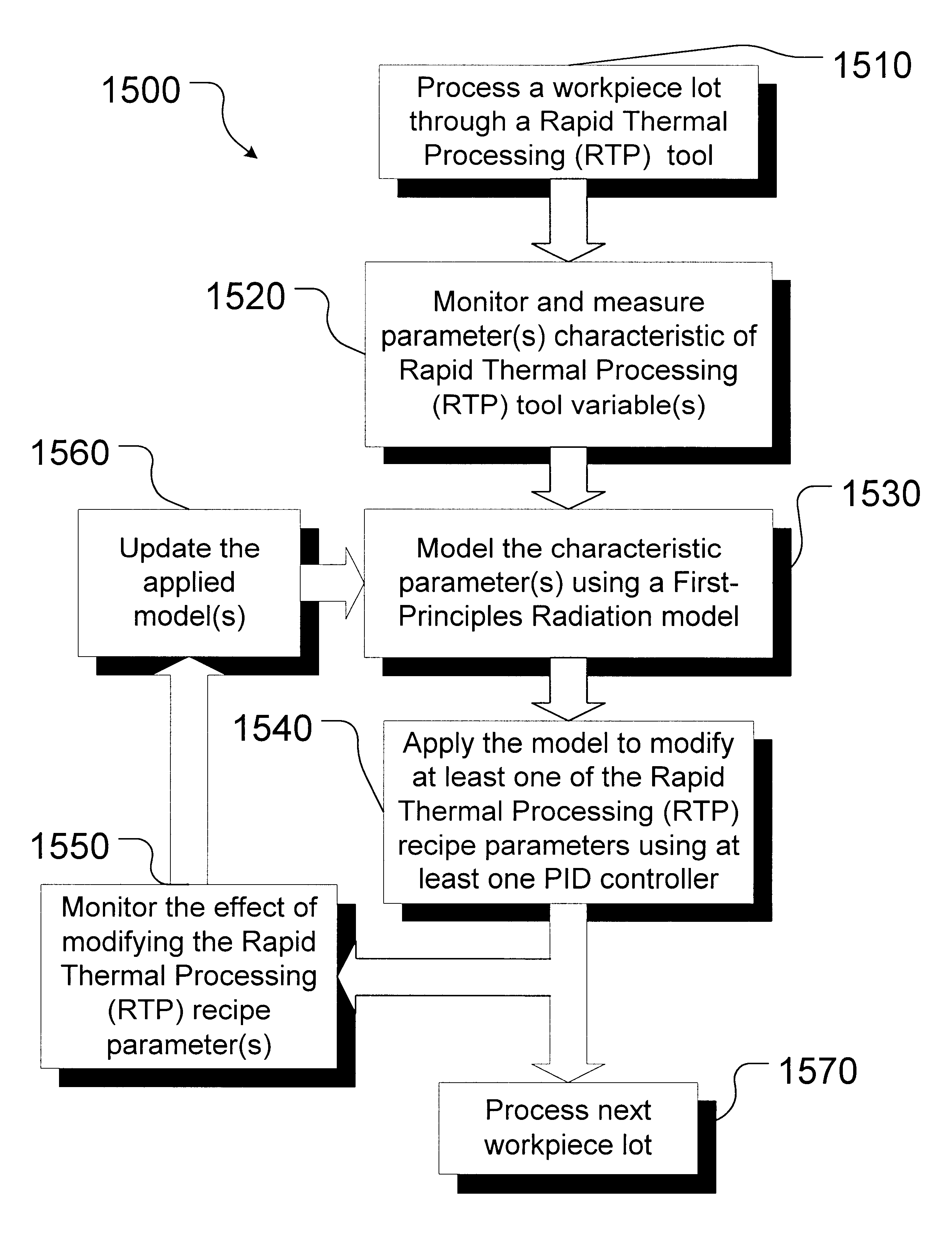
A method is provided, the method comprising measuring at least one parameter characteristic of rapid thermal processing performed on a workpiece in a rapid thermal processing step, and modeling the at least one characteristic parameter measured using a first-principles radiation model. The method also comprises applying the first-principles radiation model to modify the rapid thermal processing performed in the rapid thermal processing step.

Description

1. Field of the InventionThis invention relates generally to semiconductor fabrication technology, and, more particularly, to a method for semiconductor fabrication supervision and optimization.2. Description of the Related ArtThere is a constant drive within the semiconductor industry to increase the quality, reliability and throughput of integrated circuit devices, e.g., microprocessors, memory devices, and the like. This drive is fueled by consumer demands for higher quality computers and electronic devices that operate more reliably. These demands have resulted in a continual improvement in the manufacture of semiconductor devices, e.g., transistors, as well as in the manufacture of integrated circuit devices incorporating such transistors. Additionally, reducing defects in the manufacture of the components of a typical transistor also lowers the overall cost per transistor as well as the cost of integrated circuit devices incorporating such transistors.The technologies underlyi...

Claims


Application Information

Patent Timeline
Patent Type & Authority Patents(United States)
IPC IPC(8): G05B13/04G05B11/42
CPCG05B13/042G05B11/42
Inventor RILEY, TERRENCE J.CAMPBELL, WILLIAM JARRETT
Owner ADVANCED MICRO DEVICES INC
Why Eureka
Try Eureka