Nitride semiconductor device

a technology of nitride and semiconductor, which is applied in the direction of semiconductor devices, semiconductor lasers, semiconductor lasers, etc., can solve the problems of insufficient luminous intensity of conventional led devices, easy damage of devices made of nitride semiconductor, and insufficient availability of led devices with higher luminous intensity. achieve good electrostatic withstanding voltage and improve luminous intensity

Inactive Publication Date: 2005-01-04
NICHIA CORP
View PDF22 Cites 59 Cited by
  • Summary
  • Abstract
  • Description
  • Claims
  • Application Information

AI Technical Summary

Benefits of technology

[0010]The first object of the present invention is to provide a First nitride semiconductor light emitting device with an active layer of the multiple quantum well structure, in which the device has an improved luminous intensity and a good electrostatic withstanding voltage, thereby allowing the expanded application to various products.

Problems solved by technology

However the luminous intensity of the conventional LED device is not enough for use as a light source of a illumination lamp and / or a outside display exposed to direct sunshine.
It has been long felt needed that the light emitting device having an active layer of quantum well structure will be improved in its luminous intensity, but such a LED device with higher luminous intensity has not yet been available.
Also, the device made of nitride semiconductor has a layer structure, which may be inherently be weak against the electrostatic voltage.
Thus, the device of nitride semiconductor may be easily damaged even by the electrostatic voltage of 100V which is much lower than that people can feel.
There are substantial risks of damaged device characteristics in handling the device, for example, taking it out of an antistatic bag, and assembling it to a product.

Method used


Image

  • Nitride semiconductor device
  • Nitride semiconductor device
  • Nitride semiconductor device

Examples


example 1

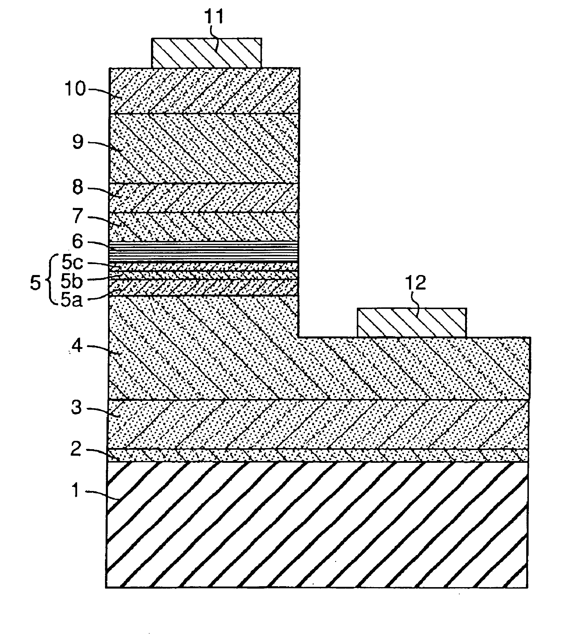
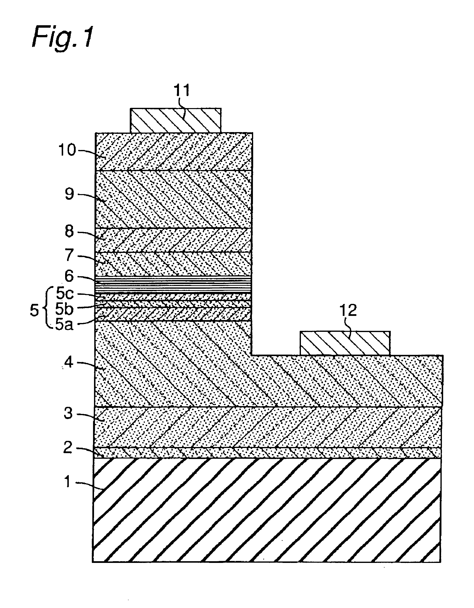
[0217]Referring to FIG. 1, Example 1 is explained hereinafter.

[0218]A substrate 1 of sapphire (C-face) is set within a MOCVD reactor flown with H2, and the temperature of the substrate is set to 1050° C., the substrate 1 is cleaned.

[0219](Buffer Layer 2)

[0220]Subsequently, the growth temperature is decreased to 510° C. and a buffer layer 2 made of GaN which has a thickness of about 100 angstroms is grown on the substrate 1 flown with H2 as a carrier gas, and NH3 and TMG (trimethylgallium) as material gases into the reactor.

[0221](Undoped GaN Layer 3)

[0222]After growing the buffer layer 2, only TMG is held, and the substrate temperature is increased to 1050° C. After the temperature is stable, again the material gas of TMG and NH3 and the carrier gas of H2 are flown into the reactor to grow the undoped GaN layer 3 having a thickness of 1.5 μm on the buffer layer 2.

[0223](n-contact Layer 4)

[0224]While the growth temperature is kept to 1050° C., the material gas of TMG and NH3, and an ...

example 2

[0242]Another LED device is manufactured, which is similar to that of Example 1 except that the active layer 7 is formed as described below. Therefore, no further explanation will be made thereto.

[0243](Active Layer 7)

[0244]The barrier film made of undoped GaN with a thickness of 250 angstroms is laminated, and after the growth temperature is set to 800° C., the material gas of TMG, TMI, and NH3, and the carrier gas of H2, are flown into the reactor to laminate a well layer made of undoped In0.3Ga0.7N with a thickness of 30 angstroms. These steps are repeated 6 times, and lastly, an another barrier layer is laminated, so that each of the well layers is sandwiched by the barrier layers on both surfaces. Thus, the active layer 7 of Example 2 is grown of the multiple quantum well structure with a thickness of 1930 angstroms.

[0245]The resultant LED device emits pure blue light with a peak wavelength of 470 nm at the forward current of 20 mA and has favorable optical and electrical chara...

example 3

[0246]Again, another LED device is manufactured, which is similar to that of Example 1 except that the active layer is formed as described below. Therefore, no further explanation will be made thereto.

[0247](Active Layer 7)

[0248]The barrier film made of undoped GaN with a thickness of 250 angstroms is laminated, and after the growth temperature is set to 800° C., the material gas of TMG, TMI, and NH3, and the carrier gas of H2, are flown into the reactor to laminate a well layer made of undoped In0.3Ga0.7N with a thickness of 30 angstroms. These steps are repeated 5 times, and lastly, an another barrier layer is laminated, so that each of the well layers is sandwiched by the barrier layers on both surfaces. Thus, the active layer 7 of Example 3 is grown of the multiple quantum well structure with a thickness of 1650 angstroms.

[0249]The resultant LED device emits pure blue light with a peak wavelength of 470 nm at the forward current of 20 mA and has favorable optical and electrical ...


PUM


Abstract

The present invention provides a nitride semiconductor light emitting device with an active layer of the multiple quantum well structure, in which the device has an improved luminous intensity and a good electrostatic withstanding voltage, thereby allowing the expanded application to various products. The active layer 7 is formed of a multiple quantum well structure containing InaGa1−aN (0≦a<1). The p-cladding layer 8 is formed on said active layer containing the p-type impurity. The p-cladding layer 8 is made of a multi-film layer including a first nitride semiconductor film containing Al and a second nitride semiconductor film having a composition different from that of said first nitride semiconductor film. Alternatively, the p-cladding layer 8 is made of single-layered layer made of AlbGa1−bN (0≦b≦1). A low-doped layer 9 is grown on the p-cladding layer 8 having a p-type impurity concentration lower than that of the p-cladding layer 8. A p-contact layer is grown on the low-doped layer 9 having a p-type impurity concentration higher than those of the p-cladding layer 8 and the low-doped layer 9.

Description

BACKGROUND OF THE INVENTION[0002]1. Technical Field of the Invention[0003]This invention relates to a light emitting device such as a light emitting diode (LED) and a laser diode (LD), a photodetector such as a solar cell and an optical sensor, and other nitride semiconductor devices used for electrical devices, for example, a transistor and a power device (which is expressed in the. formula, for instance, InXAlYGa1−X−YN, 0≦X, 0≦Y, X+Y≦1).[0004]2. Description of Related Art[0005]A nitride semiconductor device has been practically developed for use of a high luminous blue and pure green LED to fabricate light sources of a full color LED display, a traffic signal, and an image scanner. The LED device basically comprises a substrate of sapphire, a buffer layer made of GaN, an n-contact layer made of GaN doped with Si, an active layer made of a single quantum well (SQW) structure of InGaN or made of a multiple quantum well (MQW) structure containing InGaN, a p-cladding layer made of AlG...

Claims


Application Information

Patent Timeline
Patent Type & Authority Patents(United States)
IPC IPC(8): H01L33/00H01S5/323H01S5/00H01L33/02H01L33/32
CPCH01L33/025H01L33/32H01S5/32341
Inventor TANIZAWA, KOJI
Owner NICHIA CORP
Why Eureka
Try Eureka