Semiconductor device and method for manufacturing the same

a technology of semiconductor devices and semiconductors, applied in semiconductor devices, semiconductor/solid-state device details, electrical apparatus, etc., can solve the problems of affecting the affecting the growth of silicide between gate electrodes, and difficult formation of refractory metal layers, etc., to reduce the diameter of shared contacts, reduce the occurrence of defective junction leakage, and increase contact resistance

Inactive Publication Date: 2005-01-04
RENESAS ELECTRONICS CORP
View PDF8 Cites 11 Cited by
  • Summary
  • Abstract
  • Description
  • Claims
  • Application Information

AI Technical Summary

Benefits of technology

The second object of the present invention is to provide a semiconductor device that has a low-resistance silicide layer between gates even if the pitch of the gate is reduced.
The third object of the present invention is to inhibit the occurrence of defective junction leakage and increased contact resistance by optimizing shap...

Problems solved by technology

Increase in such parasitic capacity has interfered with advantages due to down sizing such as high speed and low power consumption.
This is because the formation of a refractory metal layer is difficult by methods such as sputtering, since the sidewall spacer 107 fills the space between gate electrodes 103.
Also, a problem in which the stress of the nitride film inhibits the growth of silicide between gate electrodes arises.
As a resu...

Method used


Image

  • Semiconductor device and method for manufacturing the same
  • Semiconductor device and method for manufacturing the same
  • Semiconductor device and method for manufacturing the same

Examples


first embodiment

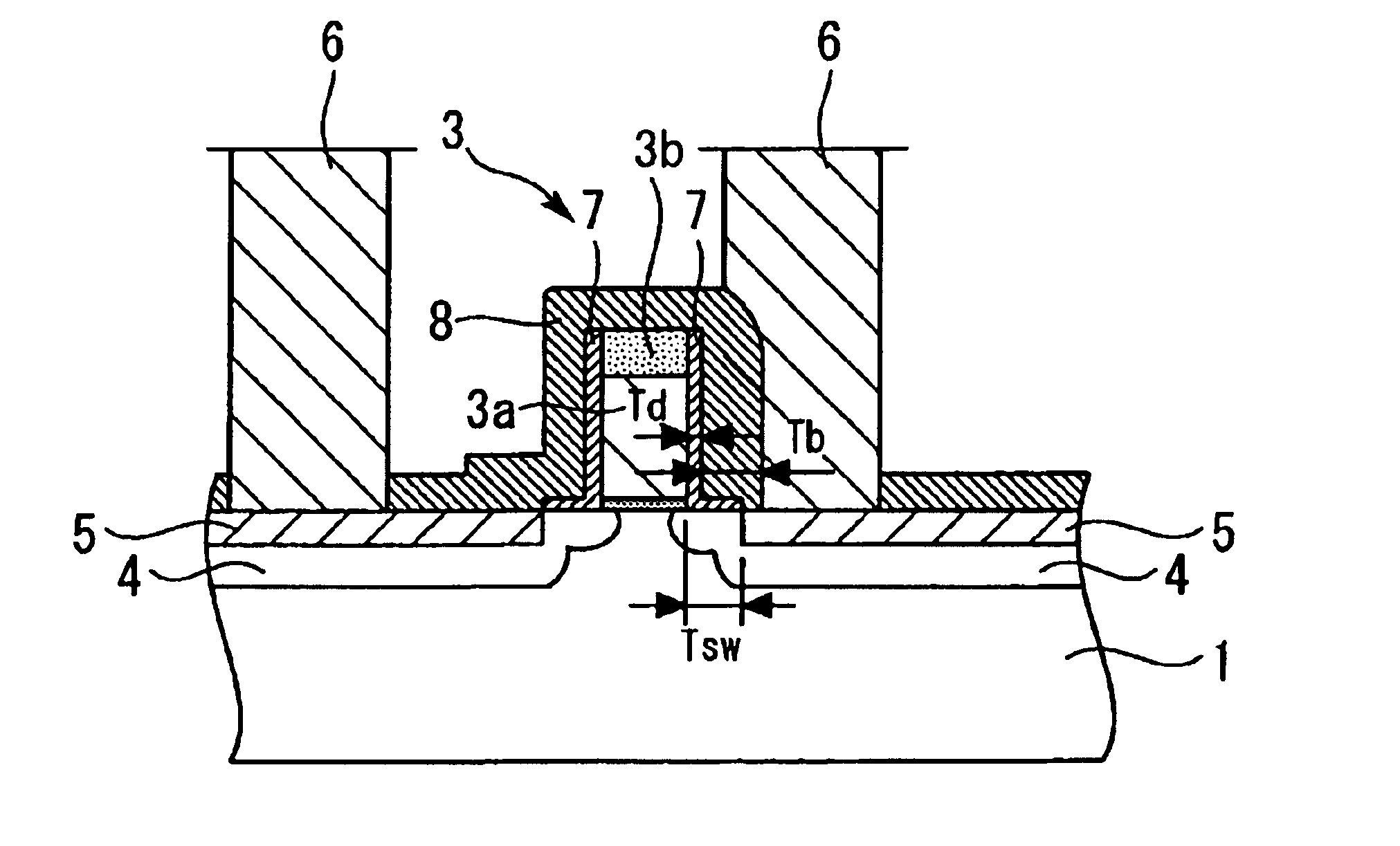
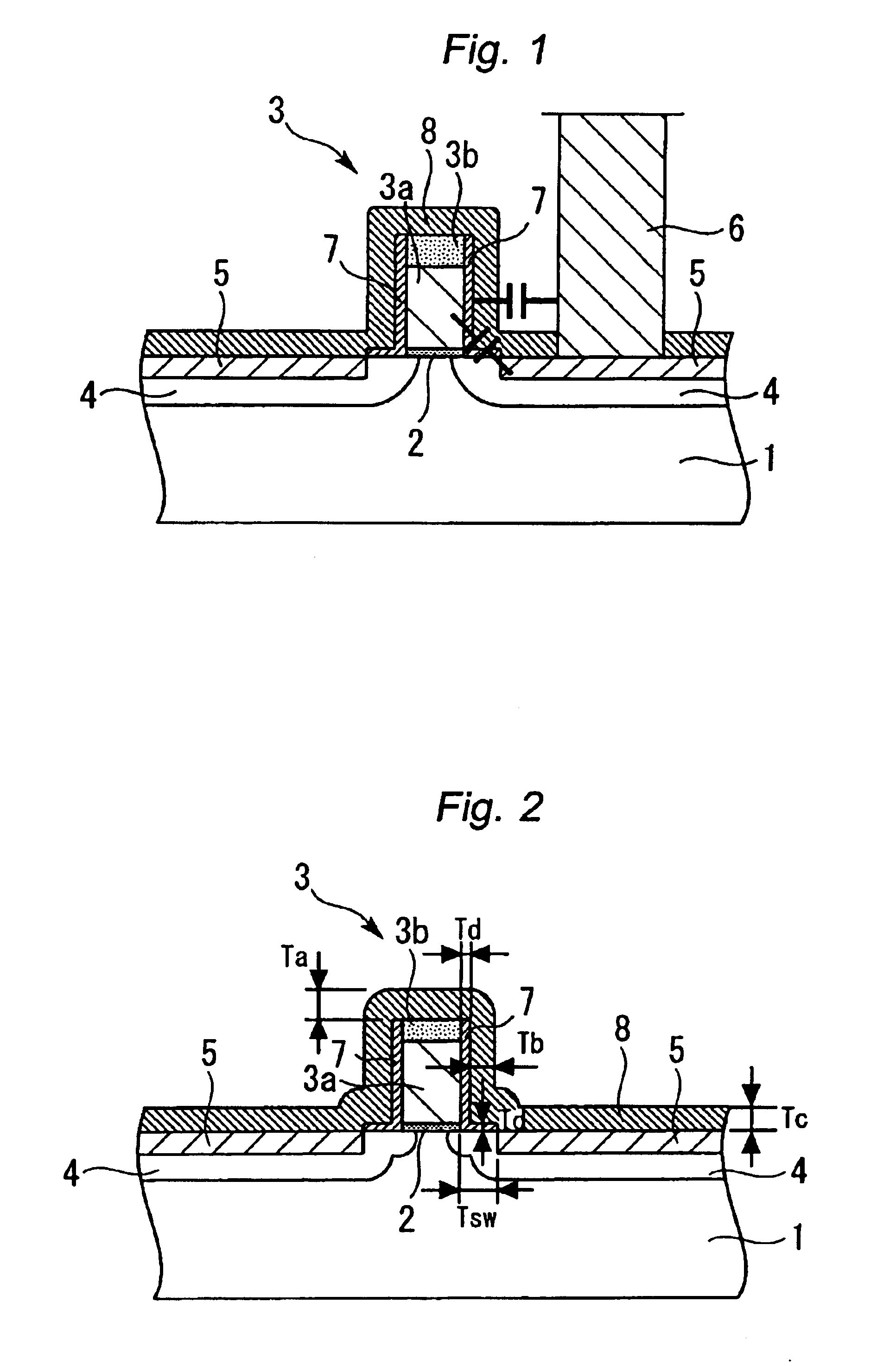
FIG. 1 is a schematic sectional view showing a semiconductor device according to First Embodiment of the present invention. The configuration of the semiconductor device of First Embodiment will be described below referring to FIG. 1. The semiconductor device of First Embodiment is an example of MOS transistors of an SAC structure to which the present invention is applied, and comprises a gate electrode 3 formed on a silicon semiconductor substrate 1 through a gate oxide film 2; a pair of impurity diffusion layers 4 of source / drain diffused layers formed on the surface region of the silicon semiconductor substrate 1 in the both sides of the gate electrode 3; a silicide film 5 formed on the surface of the impurity diffusion layers 4; and a contact electrode 6 electrically connected to the silicide film 5.

Silicon nitride films 7 are formed on the sidewalls of the gate electrode 3. These silicon nitride films 7 are formed so as to extend from the sidewalls of the gate electrode 3 to th...

second embodiment

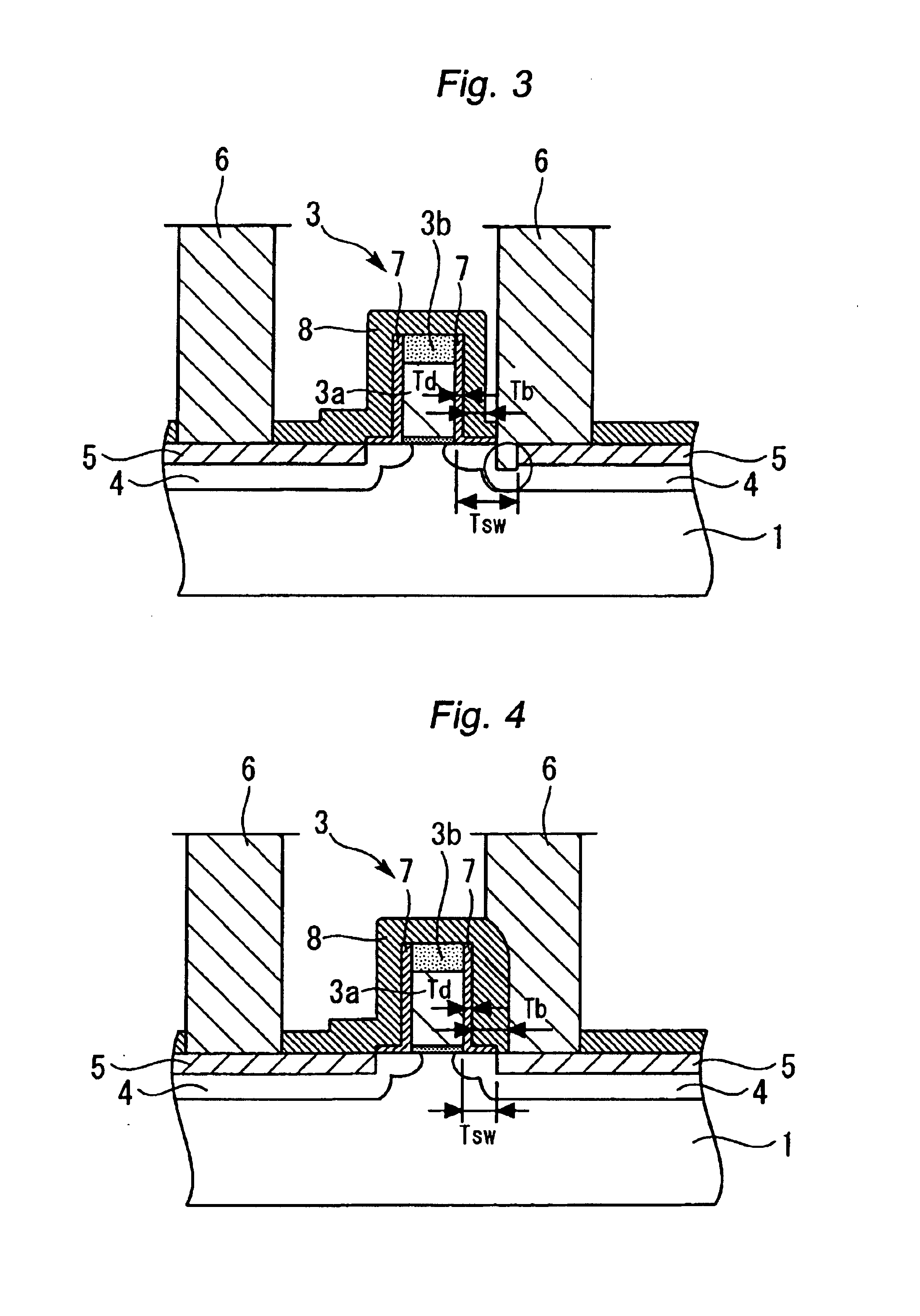
FIG. 6 is a schematic sectional view showing a semiconductor device according to Second Embodiment of the present invention. Second Embodiment shows a memory cell configuration in which a silicide film 5 is formed in an impurity diffusion layer 4 on the surface of a silicon semiconductor substrate 1 between gate electrodes 3 formed adjacent to each other. The configurations of the gate electrode 3, the silicon nitride film 7 around the gate electrode 3, and the silicon nitride film 8 are the same as those in First Embodiment.

It is very difficult to form silicide in an impurity diffusion layer surrounded by a gate electrode. The reason for this is that the sidewall spacer formed on the sidewall of the gate electrode extends laterally. In particular, if the pitch between gate electrodes is small, the formation of a refractory-metal film on the impurity diffusion layer by sputtering becomes difficult.

In the semiconductor device shown in FIG. 6, a silicon nitride film 7 of a uniform thi...

third embodiment

Next, Third Embodiment of the present invention will be described. As described referring to FIG. 19, since a shared contact for simultaneously connecting the gate and the impurity diffusion layer is suitable for the size reduction of memory cells, it is used in SRAM cells and the like that require high integration.

The semiconductor device of Third Embodiment is the semiconductor device of First Embodiment applied to a memory cell that has a shared contact. The configuration of the semiconductor device of Third Embodiment will be described below referring to FIG. 9. In FIG. 9, the configuration of gate electrodes 3, and the silicon nitride films 7 and 8 around the gate electrodes 3 is the same as the configuration of First Embodiment.

In the semiconductor device shown in FIG. 9, the silicon nitride films 8 on one surface of the impurity diffusion layer 4 are removed due to the formation of the contact hole, and the silicon nitride films 8 are also removed from the upper surface of th...


PUM


Abstract

To provide a semiconductor device with reduced parasitic capacity in the vicinity of gate electrodes, and a method for manufacturing such a semiconductor device. The semiconductor device comprises a gate electrode formed on a silicon semiconductor substrate 1 through a gate oxide film, and a pair of impurity diffusion layers formed on the surface region of the silicon semiconductor substrate at both sides of the gate electrode. A silicon nitride film acting as a sidewall spacer is formed so as to cover the sidewall of the gate electrode, and the silicon nitride film is allowed to extend to the surface of the silicon semiconductor substrate 1 in the vicinity of the gate electrode in a substantially L-shaped profile.

Description

BACKGROUND OF THE INVENTION1. Field of the InventionThe present invention relates to a semiconductor device, and a method for manufacturing the semiconductor device, specifically to the gate structure of an MOS transistor and the contact structure that contains gate wirings and LIC (local interconnect).2. Background ArtConcurrent with the size reduction of semiconductor elements, the margin of the areas for forming contacts from the upper layer to the substrate also tends to decrease. Therefore, in order to prevent the occurrence of electrical short-circuiting from the element-isolating end to the substrate when a contact is out of an active region, methods for forming contacts known as a borderless contact structure or a self align contact structure (hereafter referred to as SAC structure) are positively adopted.In the SAC structure, materials that have an etching selection ratio with a silicon oxide film often used as an interlayer insulating film are required. An example of such ...

Claims


Application Information

Patent Timeline
IPC IPC(8): H01L21/285H01L21/60H01L21/70H01L21/336H01L21/02H01L21/768H01L21/8234H01L21/8244H01L23/522H01L27/088H01L27/11H01L29/78
CPCH01L21/28518H01L21/7682H01L21/76834H01L21/76895H01L21/76897H01L21/823425H01L21/823468H01L29/6653H01L2924/0002H01L23/5222H01L2924/00
Inventor IGARASHI, MOTOSHIGEAMISHIRO, HIROYUKI
Owner RENESAS ELECTRONICS CORP
Why Eureka
Try Eureka