Method and system for probing, testing, burn-in, repairing and programming of integrated circuits in a closed environment using a single apparatus

a technology of integrated circuits and apparatuses, applied in the field of test equipment, can solve the problems of circuit device burn-in and circuit device burn-in, and the ability of conventional probe cards to contact all dice on a wafer, and achieve the effect of reducing the thickness of oxide films

Inactive Publication Date: 2005-01-04
ELM TECH
View PDF105 Cites 54 Cited by
  • Summary
  • Abstract
  • Description
  • Claims
  • Application Information

AI Technical Summary

Benefits of technology

The objects, features and advantage of the present invention will be apparent from the following detailed description in which:
will be apparent from the following detailed description in which:
FIG. 1 is a multi-functional semiconductor test and circuit configuration system according to the present invention.
FIG. 2 is one of the modules shown in FIG. 1.
FIG. 3 is a wafer having a plurality of integrated circuits.
FIG. 4 is a flow chart illustrating the steps of reducing the thickness of oxide films on the contact pads of the integrated circuits and the steps of testing, burning-in, configuring and binning the integrated circuits according to the present invention.

Problems solved by technology

Conventional probe cards do not provide the capability of contacting all the dice on a wafer at once.
Burn-in of circuit devices requires many hours of testing the devices under stressing temperature and electrical conditions.

Method used


Image

  • Method and system for probing, testing, burn-in, repairing and programming of integrated circuits in a closed environment using a single apparatus
  • Method and system for probing, testing, burn-in, repairing and programming of integrated circuits in a closed environment using a single apparatus
  • Method and system for probing, testing, burn-in, repairing and programming of integrated circuits in a closed environment using a single apparatus

Examples


Embodiment Construction

The present invention provides methods and apparatus for performing testing, burn-in, repairing, programming, and binning of integrated circuits in a closed environment using a single piece of equipment. In the following detailed description, numerous specific details are set forth such as particular hardware configurations and a flow chart to provide a thorough understanding of the present invention. It will be appreciated, however, by one having ordinary skill in the art that the present invention may be practiced without such specific details. In other instances, well-known structures and methods are not described to avoid obscuring the present invention unnecessarily.

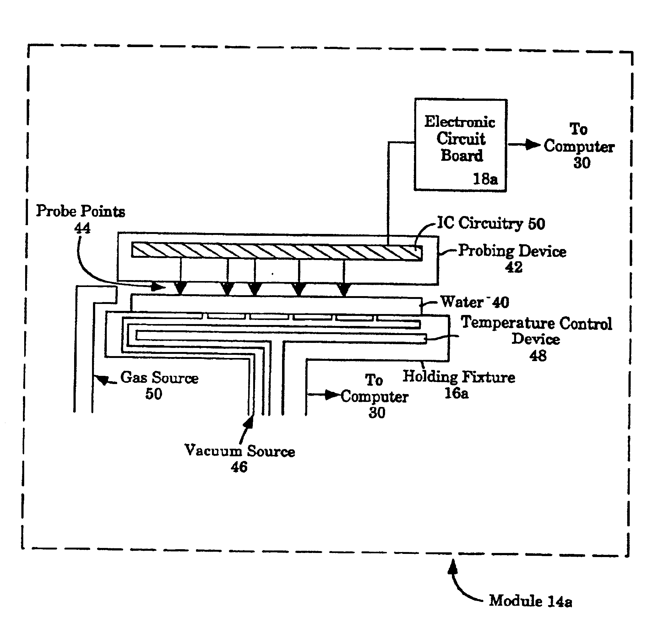
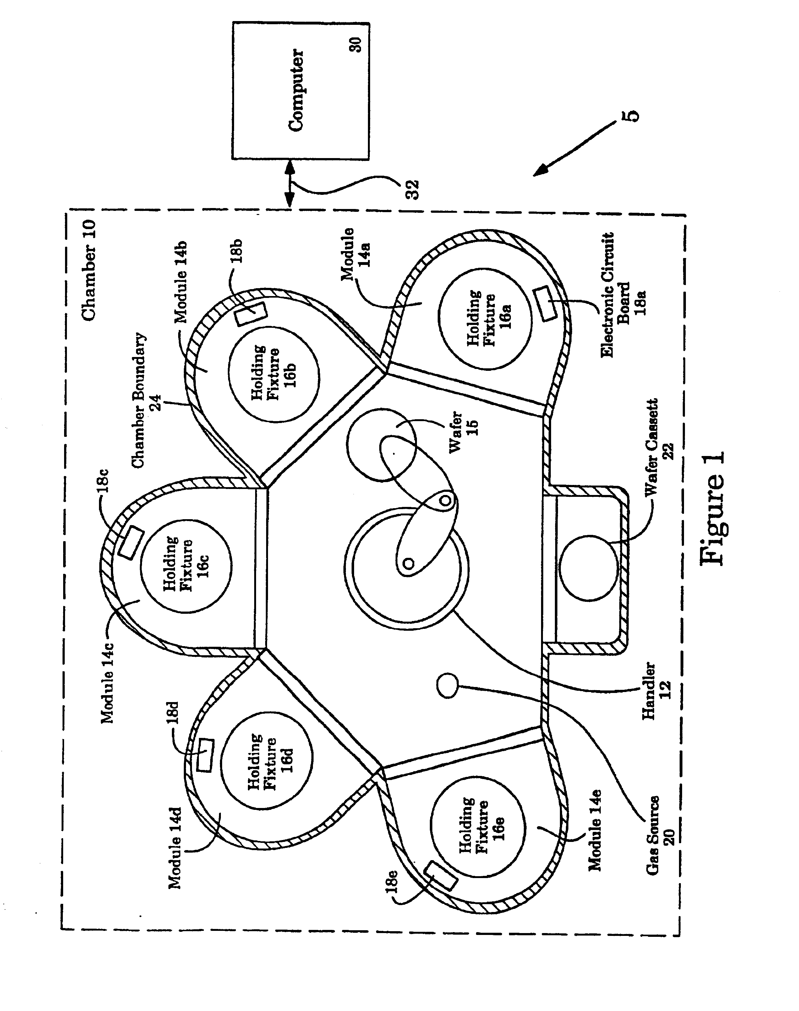
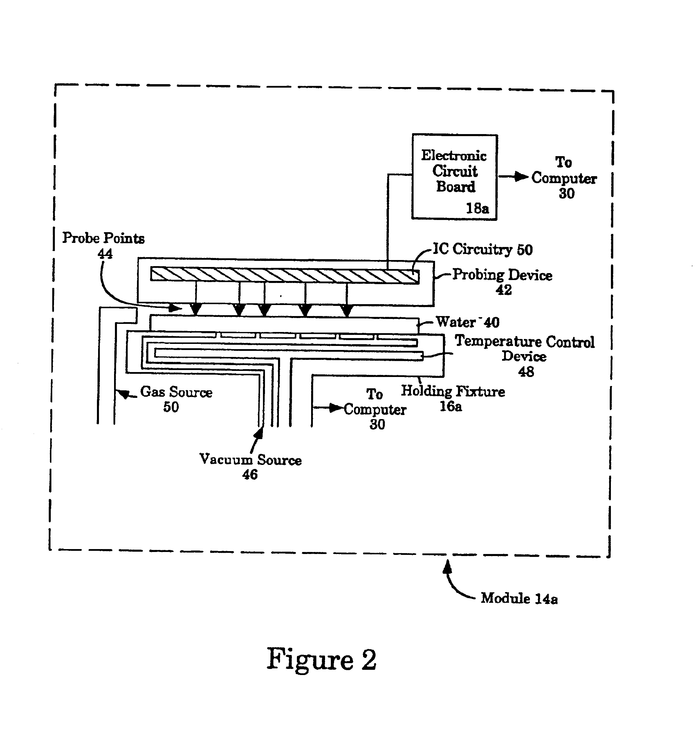
Now referring to FIG. 1, a semiconductor test and circuit configuration system 5, which is a cluster tool, is presented according to one embodiment of the present invention. System 5 includes a chamber 10 and a computer 30. Chamber 10 includes a plurality of modules 14a-14e for processing wafers, a handler 12 for mo...


PUM

PropertyMeasurementUnit
temperaturesaaaaaaaaaa
temperatureaaaaaaaaaa
thicknessaaaaaaaaaa

Abstract

A single gas tight system may perform multi-functions including reducing the thickness of oxides on contact pads and probing, testing, burn-in, repairing, programming and binning of integrated circuits. A holding fixture holds a wafer having integrated circuits and aligns the wafer to a full-substrate probing device. A temperature control device is used to heat the wafer during an oxide reduction process or during burn-in of the wafer. During the oxide reduction process, hydrogen is introduced into the chamber, and the wafer is heated so that the oxides on the contact pads can combine with hydrogen to form water vapor, thus reducing the thickness of the oxides. A computer analyzes the test and / or burn-in data and provides control signals for repairing or programming the integrated circuits.

Description

BACKGROUND OF THE INVENTION1. Field of the InventionThe present invention relates to test equipment and more particularly to equipment for probing, testing, burn-in, repairing, programming and binning of integrated circuits.2. Description of the Related ArtIn conventional semiconductor equipment technologies, separate pieces of equipment are required to test, burn-in, repair, program and bin integrated circuits (ICs). Integrated circuits that are in wafer form are tested or screened for packaging using a tungsten needle probe card, wafer positioning equipment called a prober and automatic test equipment (ATE) which supplies test signals to the probe card and determines the validity of any output signals. A probe card is a connector that provides a mechanical means for making a temporary contact to the contact pads on an IC for the purpose of testing the IC. The probe card may contact only a single die, but it may typically contact as many as eight or more dice if the dice consist of...

Claims


Application Information

Patent Timeline
Patent Type & Authority Patents(United States)
IPC IPC(8): G01R1/067G01R1/073G03F7/20G01R31/28G01R31/319G01R31/3185G01R31/316H01L21/60H01L21/762H01L21/66G11C29/00H01L25/065H01L23/538H01L23/48H01L21/70H01L23/498H01L21/764H01L21/98H01L21/02H01L23/52G02F1/13B81B3/00H01L21/677H01L21/822H01L27/04
CPCG01R1/07307G01R31/2867G01R31/2868G01R31/2874G01R31/2886G01R31/318505G01R31/318511G01R31/31905G01R31/31912G03F7/70466G03F7/70658G11C29/006H01L21/67138H01L21/67706H01L21/67721H01L21/762H01L21/76264H01L21/764H01L22/22H01L23/498H01L23/538H01L23/5381H01L23/5383H01L23/5386H01L23/5387H01L24/75H01L24/81H01L25/0652H01L25/0655H01L25/50H01L2924/01075G01R31/2806G01R31/2831G02F1/13452H01L21/76289H01L2224/75H01L2224/7565H01L2224/81801H01L2924/01013H01L2924/01033H01L2924/01038H01L2924/01082H01L2924/10329H01L2924/13091H01L2924/14H01L2924/15192H01L2924/19041H01L2924/19042H01L2924/19043H01L2924/3011H01L2924/01005H01L2924/01006H01L2924/01019H01L2924/01023H01L2924/01074G01R1/07314H01L2924/12042H01L2924/00
Inventor LEEDY, GLENN
Owner ELM TECH
Why Eureka
Try Eureka