Semiconductor device having different types of memory cell arrays stacked in a vertical direction

a technology of memory cell array and memory cell array, which is applied in the field of semiconductor memory device and data processor device, can solve the problems of increasing the cost of the device, increasing the cost, and shortening the time necessary for charging and discharging at the time of writing, erasing or reading, and achieves the effect of fast rewriting, easy production, and little increase of the memory area

Inactive Publication Date: 2005-01-04
HITACHI LTD
View PDF4 Cites 106 Cited by
  • Summary
  • Abstract
  • Description
  • Claims
  • Application Information

AI Technical Summary

Benefits of technology

Accordingly, it is an object of the invention to provide a semiconductor memory device capable of fast rewriting with little increasing of the memory area. In addition, it is ano...

Problems solved by technology

Thus, since this technique needs to provide a buffer memory as a separate chip and use a complicated control system, the cost is greatly increased as compared with the case in which only a flash memory could be used.
However, since the register occupies a large area, the chip area would be increased, and thus the cost still rises.
In addition, if the capacitance of data line is reduced simply from the view point of improving the performance of semiconductor memory devices, the time necessary for charging and discharging is short at the time o...

Method used


Image

  • Semiconductor device having different types of memory cell arrays stacked in a vertical direction
  • Semiconductor device having different types of memory cell arrays stacked in a vertical direction
  • Semiconductor device having different types of memory cell arrays stacked in a vertical direction

Examples


embodiment 1

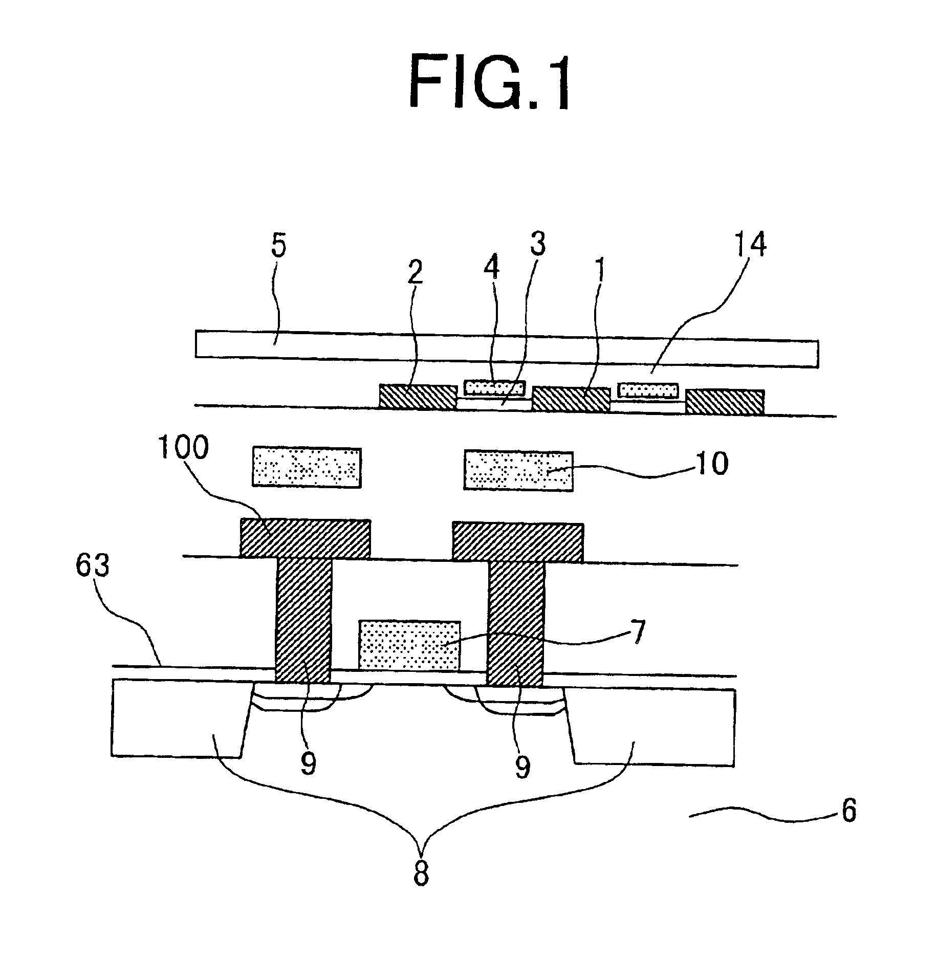
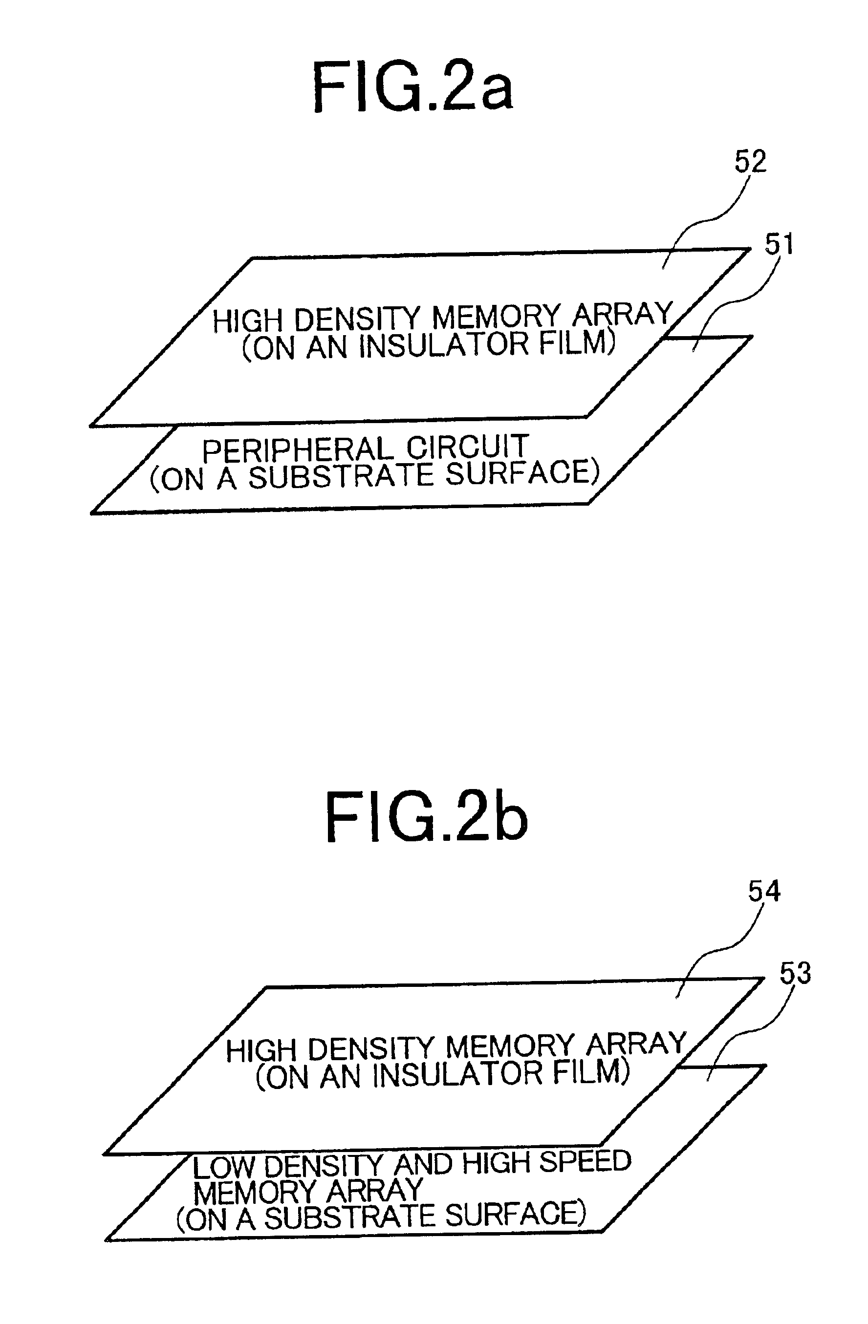
We shall describe a memory device or data processor device of the first embodiment according to the invention. FIGS. 2 are conceptual diagrams of a memory array portion of the memory device. As shown in FIG. 2a, a peripheral circuit 51 such as a sense amplifier and driver is built on a silicon substrate surface, and a memory cell array 52 is provided thereon with an insulator film interposed therebetween. According to this construction, a small-area memory device can be produced as compared with the case where the memory cell array and the peripheral circuit are formed on the same plane. Also, this construction is suited for fast operation because the memory cell array and the peripheral circuit can be connected by short conducting lines. The memory cell array on the insulator film is not limited to semiconductor memories, but may be memories made of other materials such as MRAM (magnetic random access memory). The MRAM stores information by utilizing a phenomenon that the resistanc...

embodiment 2

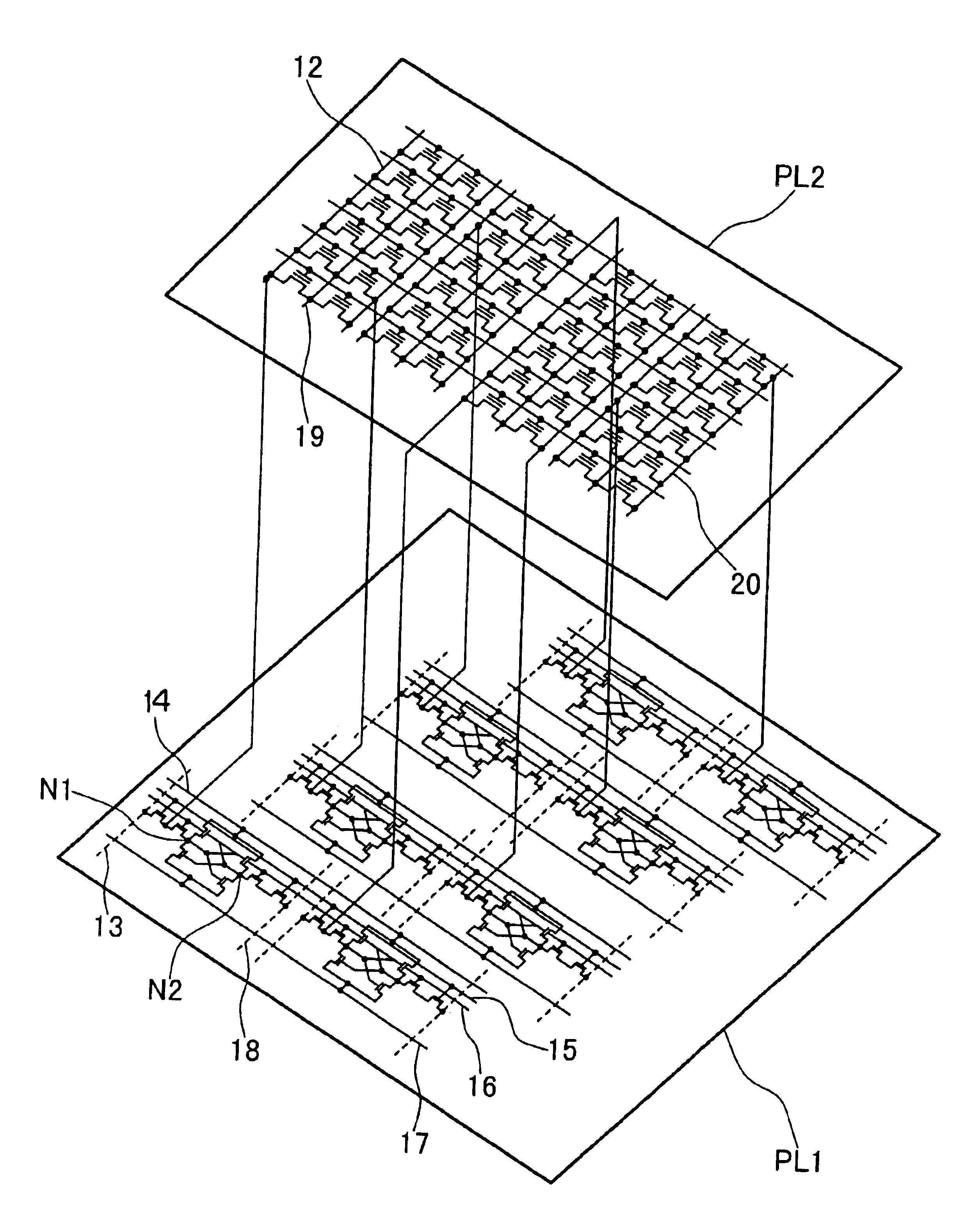
FIGS. 9, 10 and 13 show a memory device of another embodiment according to the invention. FIG. 9 is a circuit diagram of another arrangement of the SRAM cell illustrated in FIG. 8. FIGS. 10 and 13 are, respectively, a cross-sectional view of the memory and a circuit diagram of the cell array, of the flash memory portion in embodiment 1. The other portions than these constructions are the same as in embodiment 1. The difference between embodiments 1 and 2 will be described below.

In FIG. 9, a selection transistor SF is connected differently from the transistor SL shown in FIG. 8. When the transistor SF is in the off state, this arrangement is equivalent to that of normal SRAM. Thus, it can be used not only for the function of a buffer memory for a slower, high-density integration memory as in the embodiment 1, but also genuinely for SRAM such as a secondary cache. When the high-density integration memory is accessed, switching is made to the same operation as in the embodiment 1. In t...

embodiment 3

FIG. 14 is a circuit diagram of the cell array portion of a memory device of another embodiment according to the invention. A flash memory is used for a high-density integrated memory. The interconnection of the high-density integrated memory cells is the same as in the embodiment 2. In this embodiment, unlike the embodiments 1, 2, erasing means the injection of electrons into the floating gate, and writing the extraction of the injected electrons. In addition, the high threshold corresponds to information “0”, and the low threshold to information “1”. In this embodiment, a verify circuit in addition to the sense / latch circuit in the embodiments 1, 2 is provided in each memory mat. The flash memory has a relatively large dispersion between devices about the writing and erasing characteristics as compared with DRAM and SRAM. The so-called verify operation is useful that verifies by reading after the application of write (erase) pulse, and forces the writing operation to be again perf...


PUM


Abstract

To provide a semiconductor memory device capable of fast rewriting with a small area, and/or large-capacity operation with a small area or fast operation and low power consumption operation, peripheral circuits such as logic circuit, buffer memory and sense circuit or part thereof are formed on a semiconductor substrate surface, and memory cells are provided thereon with an insulator film interposed therebetween.

Description

BACKGROUND OF THE INVENTIONThe present invention generally relates to semiconductor memory devices and data processor devices.As a conventional example concerning the present invention, there is a flash memory described in a document of IEICE Transactions, vol. E74, pp. 130-141, 1991, written by T. Masuhara et al. This flash memory cell has the source, drain and channel region formed on a silicon substrate surface, and the floating gate and control gate of polycrystalline silicon provided within an insulator. The memory function is achieved by charge accumulation within the floating gate and by use of the change of conductance between the source and drain due to the increase or decrease of the amount of accumulated charges. As another conventional example, a single-electron memory using polycrystalline silicon can be cited which is described in IEEE International Electron Circuit Conference, pp. 541-544, 1993, written by K. Yano et al, and International Solid-State Circuits Conferen...

Claims


Application Information

Patent Timeline
IPC IPC(8): G11C16/34G11C5/02G11C16/04G11C16/06H01L21/70H01L27/11H01L21/8244H01L27/115G11C11/41G11C5/06G11C11/401G11C16/02H01L21/8246H01L21/8247H01L27/00H01L27/10H01L27/105H01L29/788H01L29/792
CPCB82Y10/00H01L27/11551G11C7/24G11C16/0416G11C16/10G11C16/3454G11C16/3459H01L27/0207H01L27/0688H01L27/105H01L27/10897H01L27/11H01L27/1104H01L27/1116H01L27/115G11C5/025G11C2216/06G11C11/005H01L25/18H01L23/57H10B12/50H10B10/18H10B10/00H10B10/12H10B69/00H10B41/20G11C5/06
Inventor ISHII, TOMOYUKI
Owner HITACHI LTD
Why Eureka
Try Eureka