Light emitting device and method of manufacturing the same

Inactive Publication Date: 2005-01-18
SEMICON ENERGY LAB CO LTD
View PDF5 Cites 47 Cited by
  • Summary
  • Abstract
  • Description
  • Claims
  • Application Information

AI Technical Summary

Benefits of technology

The present invention has been made in view of the above, and an object of the present invention is therefore to provide a light emitting device in which reduction of recombinations in a light emitting element is prevented by employing a low-resistant electrode structure.
According to the present invention, a light emitting device has a light emitting element composed of first and second electrodes and an organic compound layer that is sandwiched between the first and second electrodes, and the device is characterized in that one of the first and second electrodes has a transparent conductive film, a transparent conductive resin formed on the transparent conductive film, and a plurality of conductors formed on the transparent conductive resin. The present invention obtains the effect of lowering the resistance of tile transparent conductive film by forming the plural conductors in the first or second electrode. In this specification, an electrode above the organic compound layer is called a first electrode (upper electrode) and an electrode below the organic compound layer is called a second electrode (lower electrode). The term transparent conductive resin refers to a conductive resin that has 75% or higher light transmittance, preferably, 90% or higher.
According to the present invention, a light emitting, device has a light emitting element electrically connected to a TFT, and is characterized in that an insulating, film, a transparent conductive film, a transparent conductive resin, and a plurality of conductors are formed above a gate electrode of the TFT, or above a gate wiring line connected to the TFT, or above a source wiring line connected to the TFT, or above a drain wiring line connected to the TFT, or above a current supplying line connected to the TFT, the transparent conductive film being formed on the insulating film, the transparent conductive resin being formed on the transparent conductive film, the plural conductors being formed on the transparent conductive resin. Having the above-mentioned characteristic, the present invention can reduce the resistance of the transparent conductive film without lowering the aperture ratio.

Problems solved by technology

However, the transparent conductive film has a drawback of high resistivity compared to the resistivity of a metal.
High film resistance of the anode formed of the transparent conductive film brings difficulty to injection of carriers and lowers the number of carriers that are re-combined in the light emitting element.
As a result, the light emitting element cannot emit light at a desired luminance.

Method used


Image

  • Light emitting device and method of manufacturing the same
  • Light emitting device and method of manufacturing the same
  • Light emitting device and method of manufacturing the same

Examples


embodiment 1

[Embodiment 1]

This embodiment describes the structure of a light emitting of light emitting device according to the present invention. The description is given with reference to FIG. 6.

In FIG. 6, reference symbol 501 denotes a lower electrode, which is a film of a metal such as platinum (Pt), chromium (Cr), tungsten (W), or nickel (Ni). The lower electrode 501 corresponds to an anode. The role of the lower electrode 501 in this embodiment is to inject holes to an organic compound layer when a voltage is applied. Therefore, the material of the lower electrode 501 is required to be higher in HOMO level than the organic compound that forms the orgasmic compound layer. In other words, the lower electrode is desirably formed from a material having a large work function.

Next, a hole generating layer 504 is formed by co-evaporation of an electron acceptor 502 and a low molecular weight material 503. In this embodiment, the material of the electron acceptor 502 can be the same material give...

embodiment 2

[Embodiment 2]

This embodiment describes a case of forming a mixture layer in the light emitting element of Embodiment 1. The description will be given with reference to FIG. 7.

In FIG. 7, reference symbol 601 denotes a lower electrode and 602 denotes a hole generating layer that is formed by co-evaporation of an electron acceptor and a low molecular weight material.

A hole injection layer 603, a hole transporting layer 604, a light emitting layer 605, and an electron transporting layer 606 are laminated on the hole generating layer 602 to form an organic compound layer 607. Details about the methods of forming these layers may refer to Embodiment 1.

In this embodiment, the interface between the hole transporting layer 604 and the light emitting layer 605 and the interface between the electron transporting layer 606 and the light emitting layer 605 each have a mixture layer.

In this embodiment, the mixture layer formed at the interface between the light emitting layer 605 and the hole tr...

embodiment 3

[Embodiment 3]

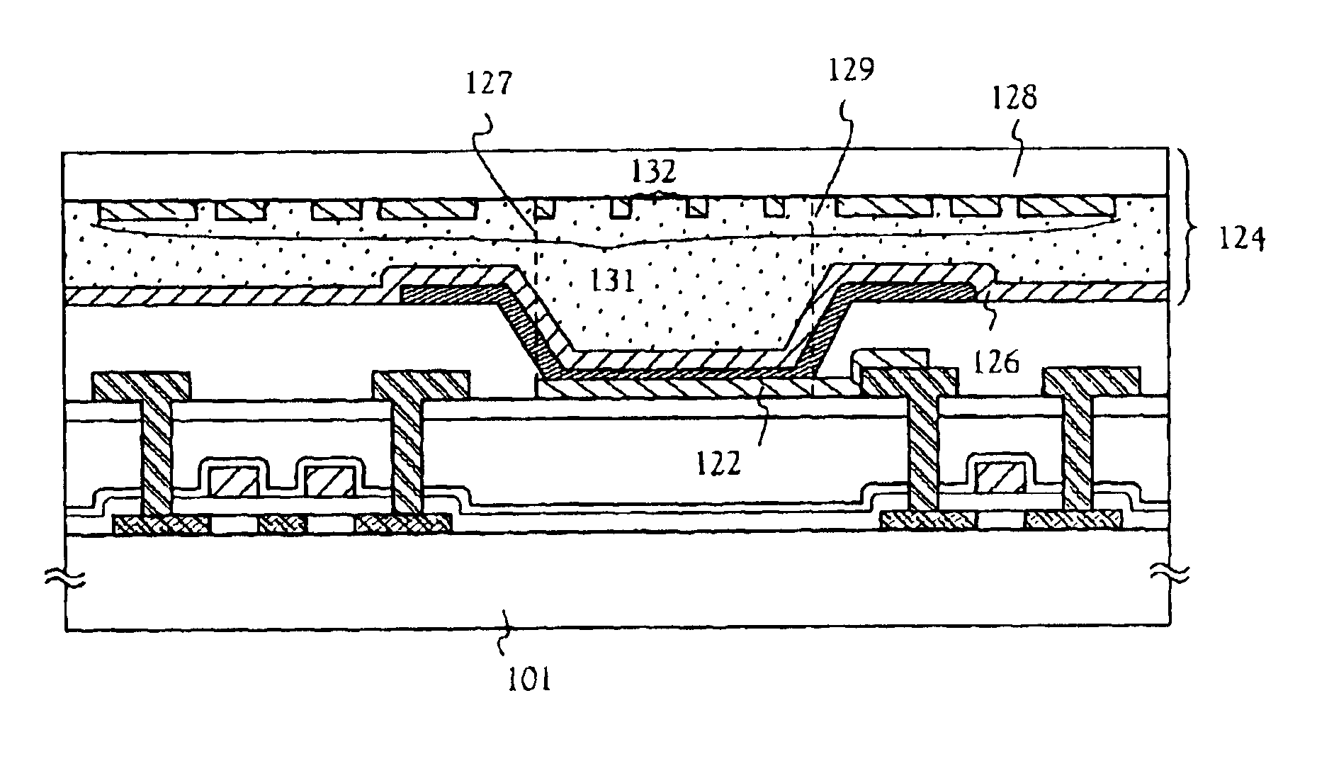
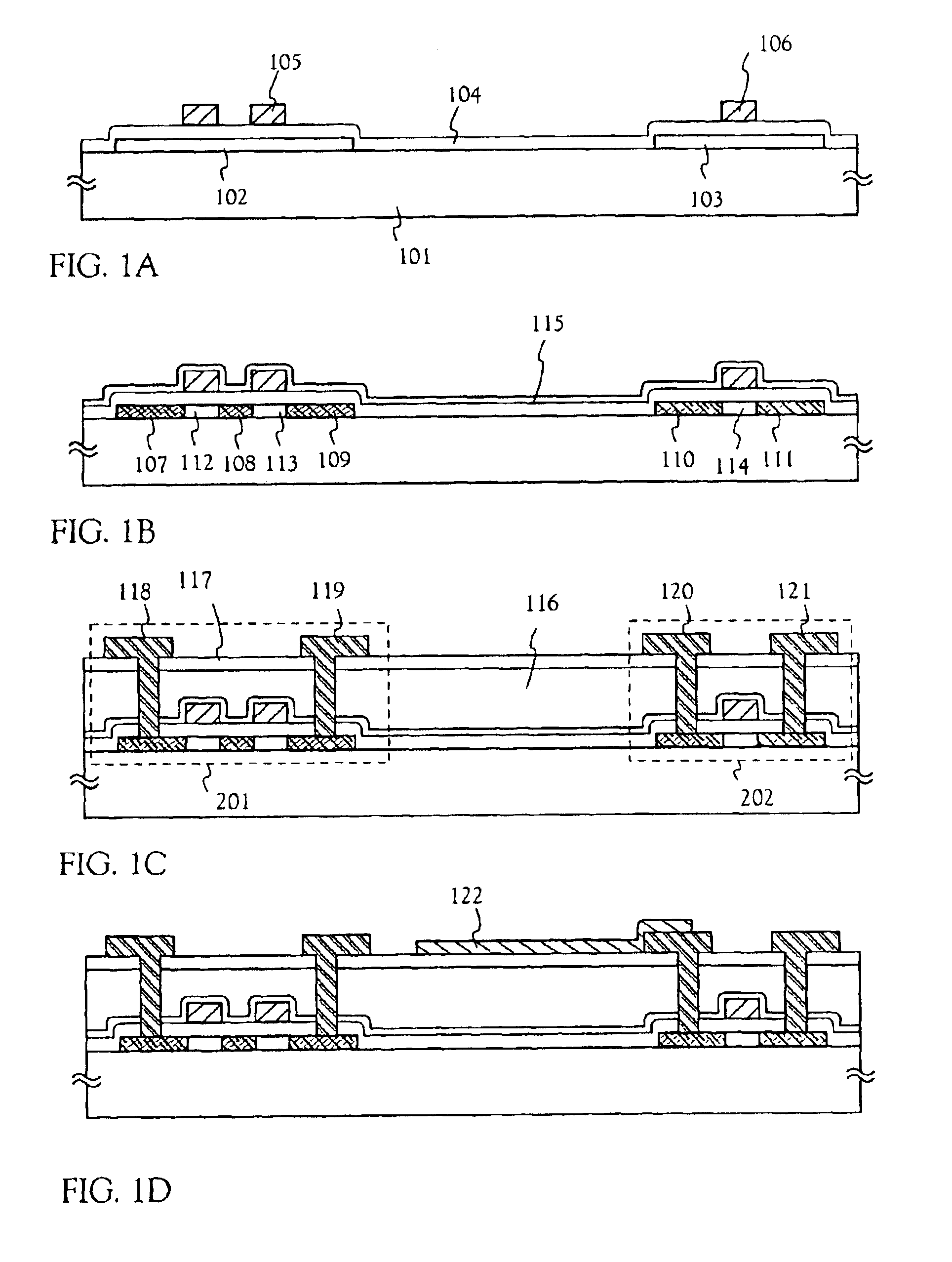
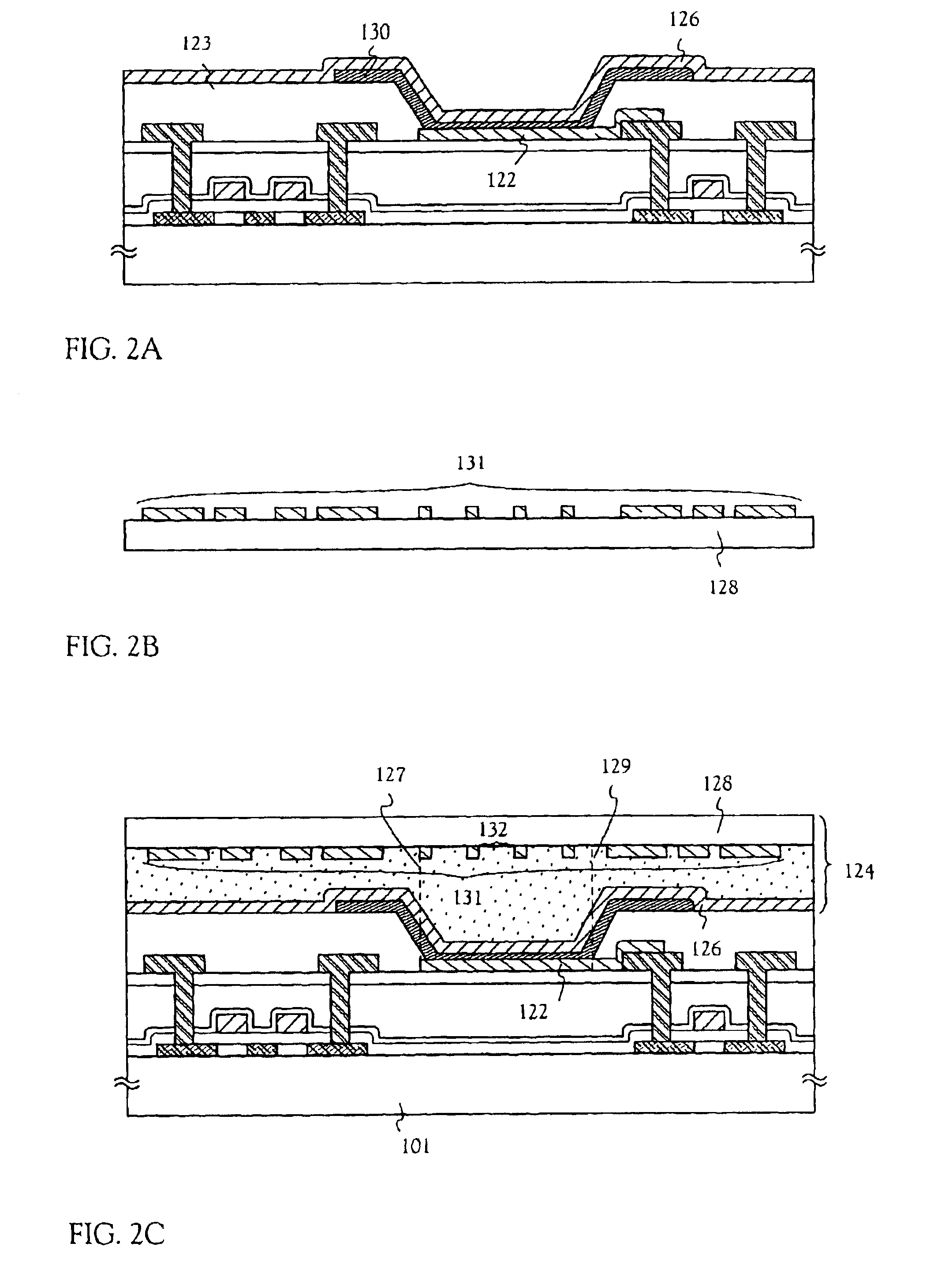
This embodiment gives a description on a light emitting device having light emitting elements that respectively emit red light, green light, and blue light. In this embodiment, a lower electrode 122 is formed as shown in FIG. 2A and then organic compound layers that emit light in different colors are formed by using different materials for their light emitting layers. All of the light emitting layers are formed by evaporation, which allows the use of metal mask in forming light emitting layers of pixels of different colors from different materials.

In this embodiment, a light emitting layer that emits light in red color (hereinafter referred to as red light emitting layer) is formed first using a metal mask. A known material can be used as the material of the red light emitting layer of this embodiment. All of the red light emitting layers to be formed in the light emitting device may be formed simultaneously. Alternatively, the red light emitting layers may be formed s...


PUM


Abstract

A light emitting device is provided in which reduction of recombinations in a light emitting element is prevented by using a low-resistant electrode structure. A light emitting device of the present invention has a light emitting element composed of first and second electrodes and an organic compound layer that is sandwiched between the first and second electrodes, and the device is characterized in that one of the first and second electrodes has a transparent conductive film, a transparent conductive resin formed on the transparent conductive film, and a plurality of conductors formed on the transparent conductive resin.

Description

BACKGROUND OF THE INVENTION1. Field of the InventionThe present invention relates to a light emitting device with a light emitting, element that has a film containing an organic compound that emits fluorescent light or phosphorescent tight upon application of electric field (the film is hereinafter referred to as organic compound layer), and to a method of manufacturing the light emitting device.In the present invention, a light emitting element is an element that has an organic compound layer between a pair of electrodes and the term light emitting device includes an image display device which uses this organic light emitting element. Also, the following modules are all included in the definition of the light emitting device: a module obtained by attaching to a light emitting element a connector such as an anisotropic conductive film (FPC: flexible printed circuit), a TAB (tape automated bonding) tape, or a TCP (tape carrier package); a module in which a printed wiring board is pro...

Claims


Application Information

Patent Timeline
IPC IPC(8): H01L51/50H01L51/52H01L27/32H01L27/28H05B33/26G09F9/30H05B33/04H05B33/10H05B33/12H05B33/22
CPCH01L51/5206H01L51/5237H01L51/5221H01L27/3244H01L2251/5315H10K59/1201H10K2102/3026H10K59/871H10K59/80524H10K50/841H10K50/813H10K50/814H10K50/816H10K50/828H10K50/846H10K59/12
Inventor YAMAZAKI, SHUNPEI
Owner SEMICON ENERGY LAB CO LTD
Why Eureka
Try Eureka