Method for fabrication of patterns and semiconductor devices

Inactive Publication Date: 2005-01-18
HITACHI LTD
View PDF13 Cites 37 Cited by
  • Summary
  • Abstract
  • Description
  • Claims
  • Application Information

AI Technical Summary

Benefits of technology

it is not possible to make use of advantageous effects of the hierarchical data, thus causing a major problem in terms of process time and data handling.
It is therefore an object of the invention to provide a method of forming patterns, utilizing an EPL-type electron beam exposure method including a proximity effect correction method capable of coping with any of forward scattering, backward scattering, including electron beam blur, and a Coulomb effect, and a method of fabricating a semiconductor device, using the method of forming patterns.
It is another object of the invention to provide a method of forming patterns, utilizing an EPL-type electron beam exposure method, based on processing enabling fast and accurate correction for the proximity effect with reference to complex LSI patterns.
It is still another object of the invention to provide a method of fabricating a semiconductor device at a low cost by utilizing an EPL-type electron beam exposure method capable of fast processing of data and handling of compressed data.
The invention as disclosed in the present specification is typically summed up hereinafter.
With the EPL-type electron beam exposure method, exposure of desired patterns can be executed in the

Problems solved by technology

As a result, deviation from design dimensions occurs to dimensions of a finished resist.
Further, there has been a problem of low throughput with electron beam lithography because it is a method whereby small patterns are exposed in sequence, however, advance has been made recently in commercial application of a method with a throughput largely improved by use of a large area mask for projection.
Consequently, it is not possible to employ a method for obtaining optimum dimensions of the patterns by varying intensity of exposure for every pattern to be exposed, which has been commonly practiced in the case of the conventional electron beam direct lithography without use of a mask for projection.
However, since it becomes necessary to execute the auxiliary exposure in addition to exposure with exposure patterns, originally intended for, there have arisen problems with this method in that a mask for the auxiliary exposure is required, and throughput is in effect decreased due to exposure to be executed twice.
Furthermore, because the auxiliary exposure results in subjecting regions other than regions of the exposure patterns to exposure, there has arisen another problem as well of inviting a drop in contrast of the deposition energy between patterned parts and unpatterned parts.
On the other hand, there has been a drawback with the method in that calculation of the dimensions of the mask pattern modification involves complex operation, requiring processing with a computer for many hours.
However, the conventional methods as described above have the following drawbacks.
Firstly, with the method of subjecting a large area en bloc to exposure, a multitude of electrons reside in an electronic optical s

Method used


Image

  • Method for fabrication of patterns and semiconductor devices
  • Method for fabrication of patterns and semiconductor devices
  • Method for fabrication of patterns and semiconductor devices

Examples


embodiment 1

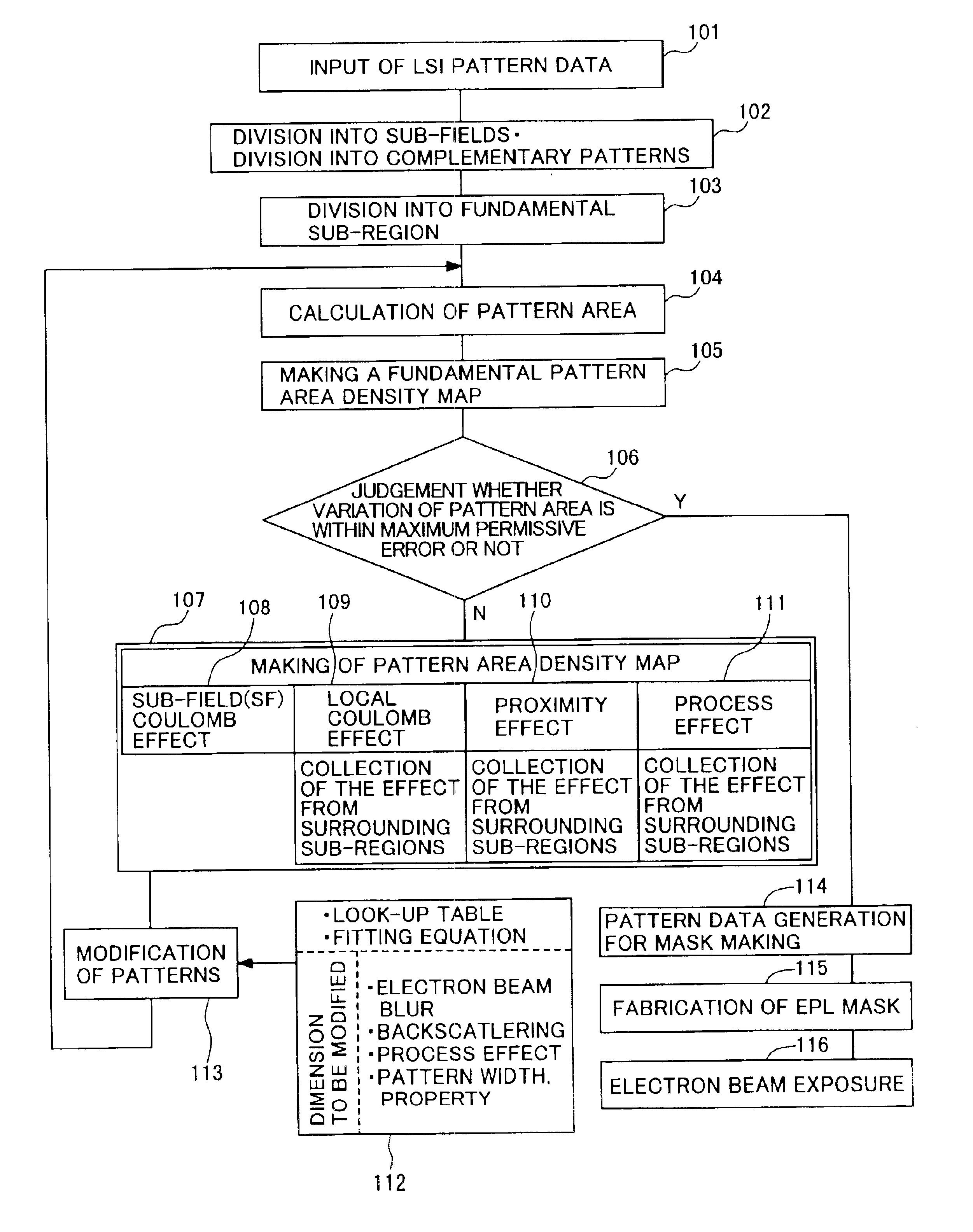
Preferred embodiments of the invention are described hereinafter with reference to FIG. 1. FIG. 1 is a flow chart illustrating a method of forming patterns. Sections in rectangular shape are function blocks for data processing. First, LSI pattern data are provided as an input (101). Subsequently, as indicated by reference numeral 102, the pattern data is divided into units of sub-field (a region of a maximum size that can be subjected to projection by an electron beam at one time, equivalent to about 250 μm square on top of a wafer) that is dependent on an electron beam lithography system. Also, depending on LSI layers, division of the data into complementary patterns is executed as necessary. The order in which division of the pattern data into the sub-fields, and division of the pattern data into the complementary patterns are executed may be reversed. Thereafter, division of the pattern data into fundamental subdivided regions to serve as units for calculation of a pattern area d...

embodiment 2

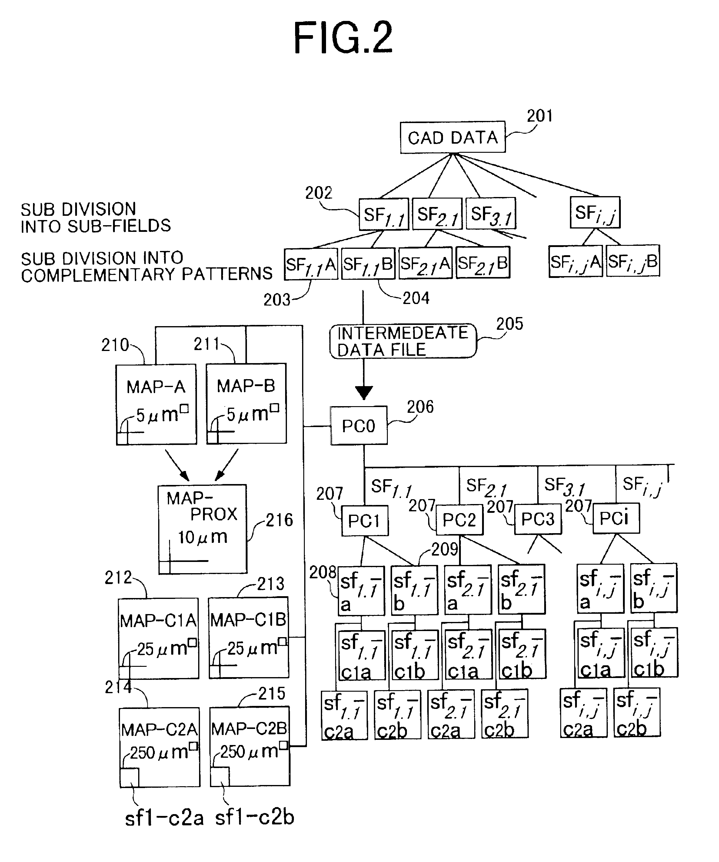
FIGS. 2 and 3 are views illustrating processing in detail in the case of dividing pattern data into complementary patterns. FIG. 2 is a view illustrating a method of finding a pattern area density map. CAD data 201 completed by a layout design for an LSI of chip size 20 mm square is first divided into those in sub-fields 202, 250 μm square. The data after division comprises 6400 sets of data, in SF1,1 to SF80,80. Subsequently, each of the sub-field data is divided into two complementary data, 203, 204, that is, divided into SF1,1 A and SF1,1 B, in the case of, for example, SF1,1. Such division is implemented such that each of the complementary data does not include a doughnut-shaped pattern therein, and a pattern has a size with a ratio of the longitudinal dimension thereof to a transverse dimension thereof (aspect ratio) not exceeding 30. Processing up to this point is outputted as a function block to an intermediate data file 205. The format of the intermediate data file is prefer...

embodiment 3

FIG. 4 is a flow chart showing a still another embodiment, illustrating a method whereby errors due to variation in pattern area density accompanying modification of patterns are reduced by means of convergence calculation, and convergence calculation is further executed at high speed. With the present embodiment, there is described only a step of modifying patterns inside a fundamental subdivided-region by use of a pattern area density map.

There exist five rectangular patterns, patterns 402 to 406, inside a fundamental subdivided region 401 of size a, shown in FIG. 4. A shorter side of the respective rectangular patterns is referred to as w1 to w5, respectively, and a longer side thereof as h1 to h5 (not shown), respectively. The pattern 402 shares a side s1 with the pattern 403, and the pattern 405 lies so as to extend into an adjacent fundamental subdivided region. A line along which the pattern 405 is intersected by a demarcation line of the fundamental subdivided region 401 is ...


PUM


Abstract

Patterns for exposure are divided into subdivided regions taking into consideration a scope of an effect of backscattering, the Coulomb effect, and process factors, respectively, on errors in dimensions, and a pattern area occupancy ratio (pattern area density) within the respective subdivided regions is retained, thereby executing exposure with patterns after finding dimensions of pattern modification as the function of the respective pattern area densities. As a result, it becomes possible to fabricate a mask provided with correction for the errors in the dimensions, caused by plural factors such as backscattering, the Coulomb effect, and process factors, and to obtain highly accurate patterns for exposure. Further, use of pattern area density maps enables data processing time necessary for correction to be considerably reduced.

Description

BACKGROUND OF THE INVENTION1. Field of the InventionThe invention relates to a method of forming fine patterns, employing a mask for projection and an electron beam, and a method for fabricating a semiconductor device, using the same.2. Description of the Related ArtWith a method of forming patterns, employing an electron beam, the electron beam with which a substrate with a resist film formed on the surface thereof is irradiated scatters inside the substrate, and returns towards the resist film on which the patterns are to be fabricated across a wide range of the resist film, thereby causing a phenomenon wherein the deposition energy of the electron beam is nonuniformly distributed depending on dimensions and disposition of patterns in the vicinity thereof. As a result, deviation from design dimensions occurs to dimensions of a finished resist. This is called a proximity effect. A range affected by the proximity effect varies depending on an acceleration voltage of an electron beam...

Claims


Application Information

Patent Timeline
IPC IPC(8): G03F7/20G03F1/16G06F17/50H01L21/02H01L21/027G03F1/20G03F1/68H01J37/302
CPCB82Y10/00B82Y40/00G03F1/144G03F1/78G03F7/2063H01J37/3026H01J37/3174G03F7/2061H01J2237/31769H01J2237/31764H01L21/027
Inventor MURAI, FUMIOFUKUDA, HIROSHI
Owner HITACHI LTD
Why Eureka
Try Eureka