Techniques for reworking circuit boards with ni/au finish

a technology of reworking circuit boards and finish, which is applied in the direction of manufacturing tools, solventing apparatus, other domestic objects, etc., can solve the problems of significant loss of added value, circuit boards may cost several thousands of dollars, and significant drawback for a company to bear the burden of regularly writing off such a cost, etc., to facilitate the containment of debris

Inactive Publication Date: 2005-01-25
EMC IP HLDG CO LLC
View PDF4 Cites 19 Cited by
  • Summary
  • Abstract
  • Description
  • Claims
  • Application Information

AI Technical Summary

Benefits of technology

One embodiment of the invention is directed to a method which includes the steps of removing original solder from the metallic pad, removing an outer portion of the metallic pad to expose an inner portion of the metallic pad, and applying new solder to the metallic pad. Removal of the original solder and the outer portion of the metallic pad exposes the inner portion which has non-corroded and non-contaminated metal. The application of new solder to this inner portion of the pad enables wettability of the pad as well as provides a protective coating to prevent corrosion of the inner portion (e.g., oxidation, reaction with contaminants, etc.).
In one arrangement, a tool has a tip which is capable of rotating. In this arrangement, the step of taking off the section of the layer of nickel includes the steps of (i) positioning the circuit board onto a workstation base, and (ii) applying the tip of the tool to the layer of nickel while the circuit board is disposed on the workstation base and while the tip of the tool rotates. Accordingly, the rotating tip can polish off (i.e., rub off, scrape off, shear off, etc.) the outer portion of nickel to expose fresh nickel.
In one arrangement, the tip of the tool includes fiber-reinforced polyester material. In this arrangement, the step of applying the tip to the nickel layer includes the step of contacting the nickel layer with the fiber-reinforced polyester material of the tip with an amount of force substantially in the range of 0.05 to 0.10 pounds of force. Accordingly, if the weight of the tool provides this amount, a technician operating the tool in a handheld manner can essentially guide the tool over the pad and allow the weight of the tool to provide the proper amount of force on the pad.
In one arrangement, the technician, prior to the step of removing the original solder from the metallic pad, draws the tip of the tool along a silicone carbide surface having a coarse grit value of substantially 160 grit (e.g., coarse grit silicon carbide paper) in order to dress the rotating the tip of the tool for removal of the original solder from the metallic pad. Such a step provides the tip with a porosity, surface finish and texture which is well-suited for removing the original solder from the metallic pad.
In one arrangement, the technician distributes carbohydroxilate flux over the metallic pad prior to removing the original solder and, again, prior to removing the outer portion of the metallic pad. The carbohydroxilate flux prevents the pad and / or the rotating tip from overheating (e.g., burning due to friction), provides a suitable amount of abrasion, and facilitates containment of debris resulting from the removal process.

Problems solved by technology

Unfortunately, there are deficiencies to the above-described conventional approaches to handling circuit boards with “Black Pad” defects.
For example, in the above-described conventional approach of simply throwing away circuit boards having “Black Pad” defects, a significant amount of added value is lost.
In particular, some circuit boards may cost several thousands of dollars to make and it may be a significant drawback for a company to bear the burden of regularly writing-off such a cost.
Additionally, the above-described second conventional approach, which involves simply removing a component and excess solder from the section of circuit board material and soldering on a new component, does not consistently and effectively repair the intermittent connections resulting from “Black Pad” defects.
Rather, these intermittent connections are often formed by flaws in the intermetallic boundaries of the nickel layers of the metallic pads, and such flaws are not fixed by simply replacing components.
To the contrary, a metallic pad suffering from a “Black Pad” defect typically has low solder-wetting ability (i.e., low affinity for solder) which does not improve when a contact of the new component is soldered to the pad.
Accordingly, any new solder joint formed on the metallic pad is likely to be unreliable.
In some situations, even if the metallic pad suffering from the “Black Pad” defect has not significantly lost its solder wetting ability, it is likely that (i) substantial nickel corrosion exists below the top surface of the metallic pad (e.g., 20 micro-inches beneath the surface) and (ii) the corrosion will remain after soldering the new component.
Thus, as long as the “Black Pad” defect remains, the circuit board will have an electrical connection which is prone to intermittent failure.

Method used


Image

  • Techniques for reworking circuit boards with ni/au finish
  • Techniques for reworking circuit boards with ni/au finish
  • Techniques for reworking circuit boards with ni/au finish

Examples


Embodiment Construction

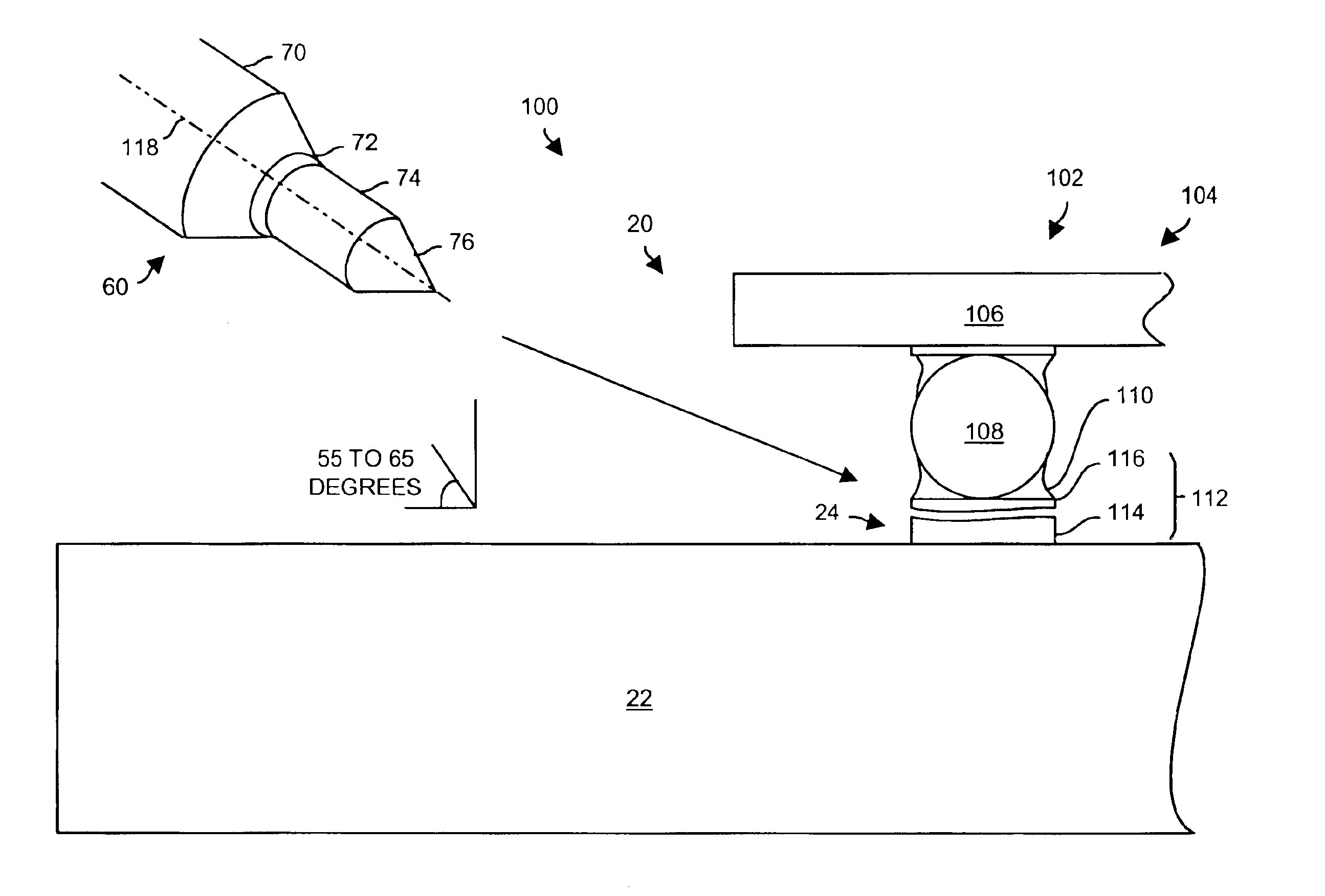
The invention is directed to techniques for reworking a circuit board having a metallic pad. The techniques involve removing an outer portion of the metallic pad to expose an inner portion of the metallic pad. These techniques are well-suited for curing “Black Pad” defects since corrosion (e.g., oxidized metal and metal reacted with other contaminants) in the outer portion of the metallic pad have been identified as significant causes of poor electrical connectivity in metallic pads suffering from “Black Pad” defects. Accordingly, removal of the outer portion of such a metallic pad exposes a healthy and reliable inner portion of the pad (i.e., fresh and uncontaminated metal) which is well-suited for establishing a new healthy electrical connection with a contact of a circuit board component.

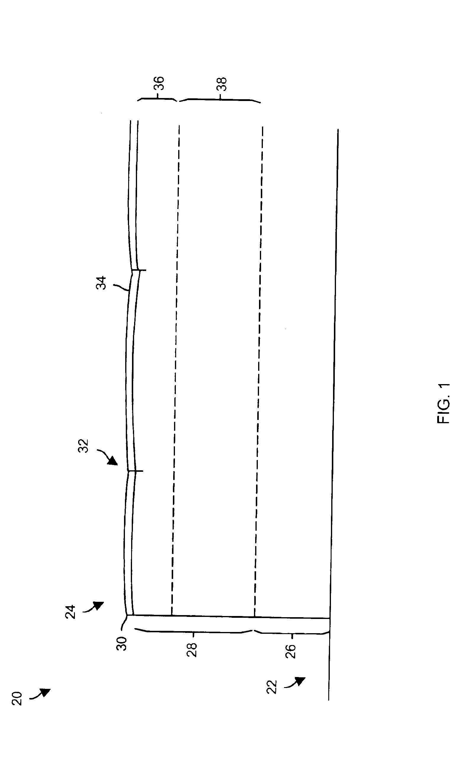
FIG. 1 shows a cross-sectional view of a portion of a circuit board 20 having a section of circuit board material 22 (e.g., conductive and non-conductive layers of material sandwiched together) a...


PUM

PropertyMeasurementUnit
timeaaaaaaaaaa
angleaaaaaaaaaa
angleaaaaaaaaaa

Abstract

Circuit board reworking techniques involve removing original solder from the metallic pad, removing an outer portion of the metallic pad to expose an inner portion of the metallic pad, and applying new solder to the metallic pad. Removal of the original solder and the outer portion of the metallic pad exposes the inner portion which has non-corroded and non-contaminated metal. The application of new solder to this inner portion of the pad enables wettability of the pad as well as provides a protective coating to prevent corrosion of the inner portion (e.g., oxidation, reaction with contaminants, etc.). Accordingly, circuit board abnormalities such as “Black Pad” defects can be cured.

Description

BACKGROUND OF THE INVENTIONA typical printed circuit assembly (PCA) includes a section of circuit board material (i.e., layers of conductive and non-conductive material sandwiched together) and one or more components attached thereto. Examples of circuit board components include integrated circuits (ICs), resistors, capacitors, connectors and pins. Some circuit board components such as Ball Grid Array (BGA) devices, Chip-Scale Packaging (CSP) devices, Flip Chip devices and Multi-chip modules (MCMs) solder to metallic pads of circuit boards using Surface Mount Technology (SMT).A typical metallic pad on the section of circuit board material includes a layer of copper, a layer of nickel and a coating of gold. Such a pad is typically formed using an electroless Nickel immersion gold surface finish process. The layer of copper is essentially an extension of the metallic etch (i.e., a trace) that runs between different locations of the section of circuit board material (e.g., to connect m...

Claims


Application Information

Patent Timeline
Patent Type & Authority Patents(United States)
IPC IPC(8): H05K3/22H05K3/04H05K3/34H05K3/02H05K3/24
CPCH05K3/225H05K3/043H05K3/244H05K3/3457H05K2201/10734Y10T29/49121Y10T29/49144Y10T29/49142Y10T29/53283Y10T29/49419H05K2203/176
Inventor LIANG, JIN
Owner EMC IP HLDG CO LLC
Why Eureka
Try Eureka