Low temperature solder chip attach structure

a low temperature, solder chip technology, applied in the direction of sustainable manufacturing/processing, semiconductor/solid-state device details, final product manufacturing, etc., can solve the problems of high cost of fabrication, inability to meet the requirements of high-temperature solder chip requirements, etc., to achieve the effect of increasing the reliability of the connection

Inactive Publication Date: 2005-01-25
INVENSAS CORP
View PDF29 Cites 21 Cited by
  • Summary
  • Abstract
  • Description
  • Claims
  • Application Information

AI Technical Summary

Benefits of technology

The present invention provides a process and structure for increasing the reliability of the connection between an area array package and a supporting su...

Problems solved by technology

The industry has moved away from the use of pins as connectors for electronic packaging due to the high cost of fabrication, the unacceptable percentage of failed connections which require rework, the limitations on input/output (I/O) density, and the electrical limitations of the relatively high resistance connectors.
Solder mounting is not a new technology.
One of the major drawbacks of this configuration is that the solder balls do not always remain in place before connection, during processing, or upon rework.
There is no guarantee, therefore, that the solder will remain associated with the...

Method used


Image

  • Low temperature solder chip attach structure
  • Low temperature solder chip attach structure
  • Low temperature solder chip attach structure

Examples


first embodiment

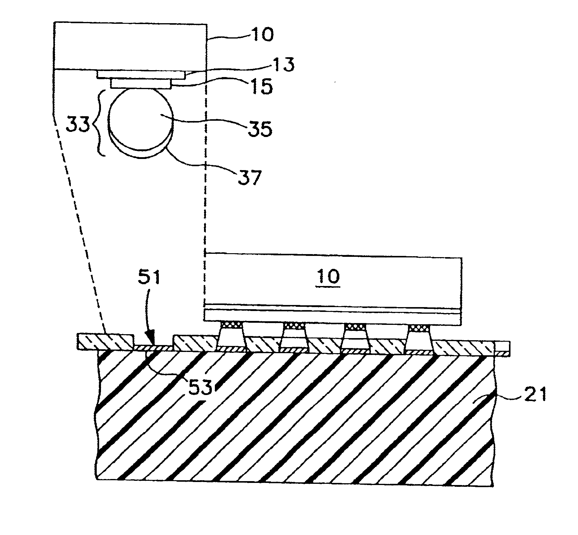
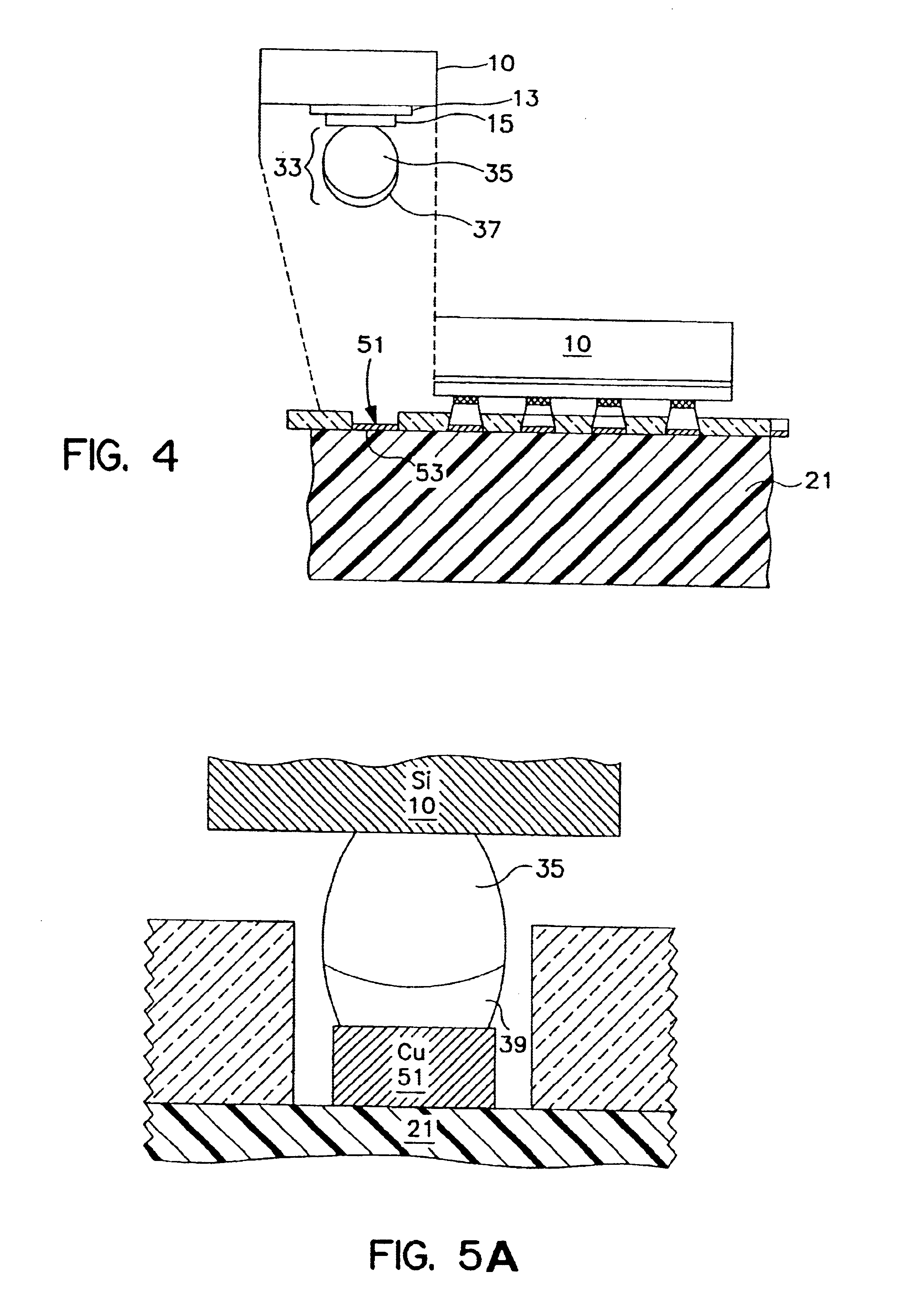
The structure of an integrated circuit (IC) chip 10 and a microelectronic circuit card 21 of the present invention is shown in FIG. 4. FIG. 4 is a cutaway view of an IC chip 10 and card 21 with a nonreflowed solder assembly 33, and a land 53 on which an adhesion or joining pad 51, preferably copper (Cu), is placed. The solder assembly 33 comprises a low melting point cap 37 formed atop a high melting point ball 35. The low melting point cap is preferably Sn, but other low melting point materials such as indium or bismuth can be used.

The high melting point ball 35, preferably Pb-rich, is deposited on solder wettable input / output (I / O) terminals 15 of an IC chip 10 or a chip carrier or other substrate. The Pb-rich balls are formed by a conventional process and affixed to the IC chip 10 in a conventional manner. A thin cap of Sn 37 is formed on the end of the ball 35. The Sn cap 37 can be applied to the Pb-rich ball 35 using any conventional process. The thickness of the cap 37 is pref...

second embodiment

the present invention is shown in FIG. 6. In FIG. 6, the Pb-rich ball 35 is attached to the IC chip 10 as in the first embodiment, but the ball 35 does not have a thin Sn cap layer. Instead, a thin layer of Sn 48 is formed on the Cu pad 51 on the land 53. The IC chip 10 with the ball 35 is brought into contact with the Sn layer 48 on the Cu pad 51 on the land 53 and heated to form the eutectic alloy. In other words, a thin Sn cap layer can be deposited onto the PCB contact and the Pb-rich ball (without the Sn cap layer) is pressed against the PCB contact. After the eutectic is formed, annealing is performed, preferably at 150° C. for 4-5 hours, to diffuse Sn into the Pb to increase the melting point of the cap layer of the resultant assembly, thus avoiding further unwanted melting during subsequent processing. Depending on the process parameters, some of the Sn may not be consumed in the eutectic and there may be a thin, high-percentage Sn layer (not shown) remaining between the eut...


PUM

PropertyMeasurementUnit
Lengthaaaaaaaaaa
Lengthaaaaaaaaaa
Temperatureaaaaaaaaaa

Abstract

A solder interconnection uses preferably lead-rich solder balls for making a low temperature chip attachment directly to any of the higher levels of packaging substrate. After a solder ball has been formed using standard processes, a thin cap layer of preferably pure tin is deposited on a surface of the solder balls. An interconnecting eutectic alloy is formed upon reflow. Subsequent annealing causes tin to diffuse into the lead, or vice versa, and intermix, thereby raising the melting point temperature of the cap layer of the resulting assembly. This structure and process avoids secondary reflow problems during subsequent processing.

Description

FIELD OF THE INVENTIONThe present invention relates in general to a process and structure for adhering a material to a supporting substrate. In particular, the present invention describes a fabrication process and structure for attaching a chip or other substrate having a ball grid array to a chip carrier or printed circuit board.BACKGROUND OF THE INVENTIONAn electronic circuit contains many individual electronic circuit components, e.g., thousands or even millions of individual resistors, capacitors, inductors, diodes, and transistors. These individual circuit components are interconnected to form circuits, and the circuits are interconnected to form functional units. Microelectronic packages, such as chips, modules, circuit cards, circuit boards, and combinations thereof, are used to protect, house, cool, and interconnect circuit components and circuits.Within a single integrated circuit (IC), circuit component to circuit component and circuit to circuit interconnection, heat diss...

Claims


Application Information

Patent Timeline
IPC IPC(8): B23K35/26B23K31/02H01L21/02H01L21/60H05K3/34B23K35/14
CPCB23K31/02H01L24/11H01L24/81H05K3/3436B23K35/268H01L2924/014H01L2224/13099H01L2224/13111H01L2224/13609H01L2224/16H01L2224/81801H01L2924/01029H01L2924/01049H01L2924/01051H01L2924/01077H01L2924/01078H01L2924/01079H01L2924/01082H01L2924/01322H01L2924/14H01L2924/19041H01L2924/19042H01L2924/19043H05K3/3463H05K2203/0435H05K2203/1105H01L2924/01005H01L2924/01006H01L2924/01024H01L2924/0105H01L2224/05001H01L2224/05027H01L2224/05022H01L2224/0508H01L2224/05572H01L24/05Y02P70/50
Inventor MILEWSKI, JOSEPH M.WOYCHIK, CHARLES G.
Owner INVENSAS CORP
Why Eureka
Try Eureka