Replication and transfer of microstructures and nanostructures

a microstructure and nanostructure technology, applied in the field of microstructure and nanostructure replication and transfer, can solve the problems of optical imaging techniques not having the same resolution as e-beam systems, the typical throughput of an e-beam machine is very slow, and the process is generally slow and impractical for large numbers of microstructures, etc., to facilitate the transfer of patterns

Inactive Publication Date: 2005-02-01
THE BOARD OF TRUSTEES OF THE LELAND STANFORD JUNIOR UNIV
View PDF3 Cites 307 Cited by
  • Summary
  • Abstract
  • Description
  • Claims
  • Application Information

AI Technical Summary

Benefits of technology

Once the template is attached to the carrier, the carrier can be stored until it is required for manufacturing. At that time, it is aligned to the final device substrate and facilitates the transfer of the pattern. The template may be adhered to the surface directly or may be applied using a form of imprint lithography. However, the key element of our invention is that the template is actually transferred to the substrate and the carrier removed, leaving the template on the substrate for subsequent processing. The template is destroyed by this subsequent processing.
With inexpensively made templates, this disposable template technique offers all the advantages of nanoimprint lithography, while eliminating the problems that occur through template reuse. Once the template is created, however, it is clear that additional processing can take place on the template prior to the transfer. This can be as simple as coating to aid in a possible subsequent transfer or nanoimplint process, or the application of coatings to allow the template itself to become a optical component such as a polarizer or fresnel lens.

Problems solved by technology

Although E-beam lithography can produce extremely high resolution patterns, the typical throughput of an E-beam machine is very slow.
Beams must be directed to each spot on the wafer in sequence, which makes the process generally slow and impractical for large numbers of microstructures.
However, optical imaging techniques do not have the same resolution as E-beam systems, and fabricating nanostructures (features with dimensions on the order of 100 nm or smaller) in these layers has been growing exponentially more expensive.
A drawback to these techniques is that the master must be repeatedly used again and again in the formation of the desired material.
This can lead to damage to the master through normal wear and exposure to contaminants.
This approach suffers from throughput limitations requiring vacuum depositions on the master.
With this approach, the master suffers degradation only from the creation of multiple replicas; the replicas themselves are used in the actual fabrication process and are discarded when damaged.
Some of the problems with PDMS as a template that limit its applicability include limited resolution (about 200 nm) because of the difference in thermal expansion coefficient between the PDMS and the mold material, and limited throughput because of the time needed for curing.
It also suffers from material incompatibility since it will stick to large areas of clean silicon.
There can be undesirable consequences from using these techniques.
For example, the definition of a particular layer with extremely fine structures with E-beam exposure will inherently risk irradiating the underlying layers to the electron beam as well.
Keeping the master or replica free of defects as it is used again and again can also present problems.
Furthermore, processing the wafer itself layer by layer, although the standard fabrication technique for integrated circuits, may be less than optimal.
For example, a metal or polysilicon layer may be best processed at a high temperature for the best results, but this degree of heating may damage or even melt the layers previously prepared on the substrate.
Because all subsequent steps in the manufacture of the microdevice are deposited on the same substrate, however, these problems in process compatibility and their required compromises remain.
Clearly, forcing a large object such as an automobile bumper to fit through a printing and patterning process to attach a simple humorous message would be awkward and very expensive.
Furthermore, although the previously disclosed molecular transfer lithography technique addresses some of these issues, the latent image formed was generally flat and did not have topographic structures corresponding to the topography desired on the final wafers.

Method used


Image

  • Replication and transfer of microstructures and nanostructures
  • Replication and transfer of microstructures and nanostructures
  • Replication and transfer of microstructures and nanostructures

Examples


Embodiment Construction

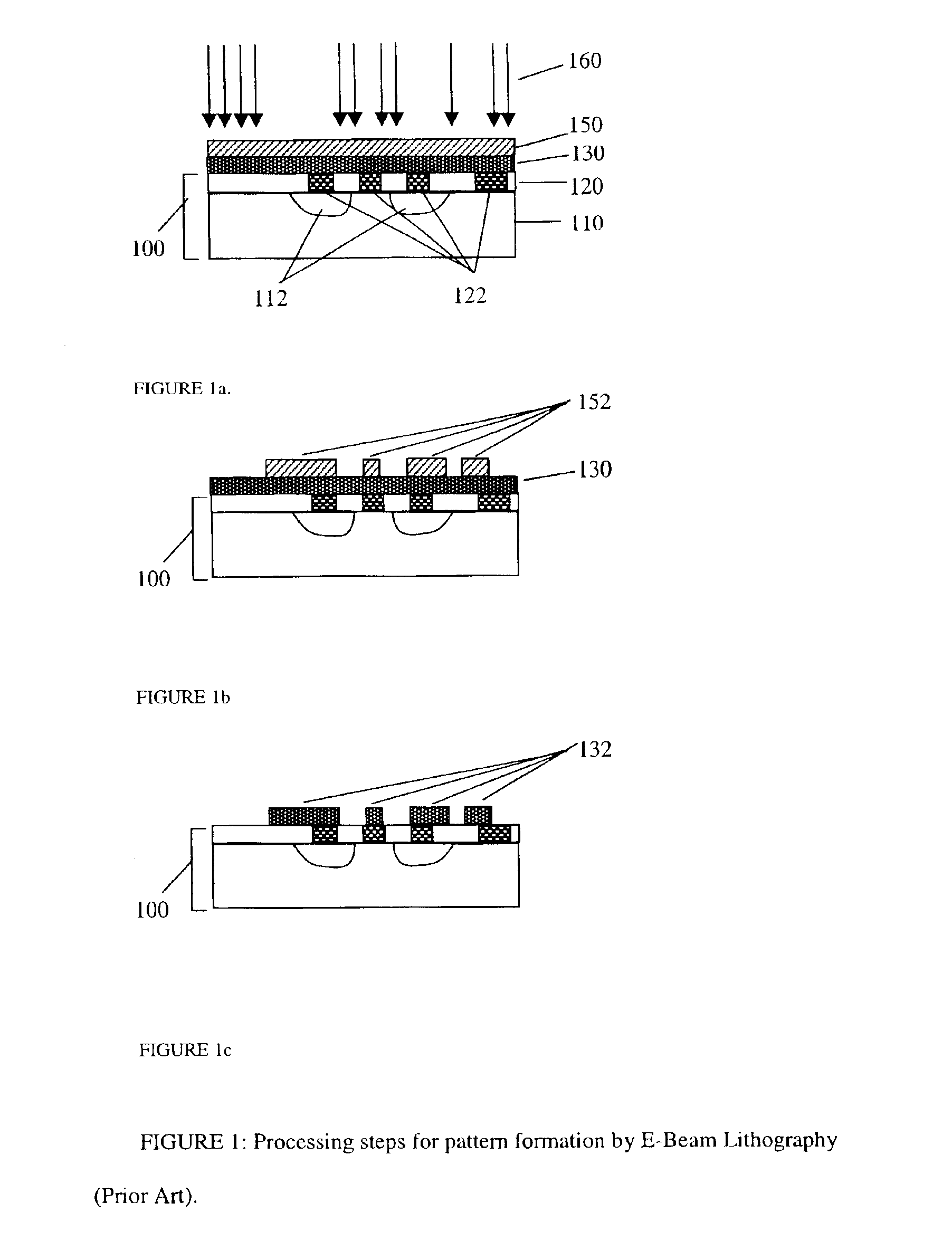
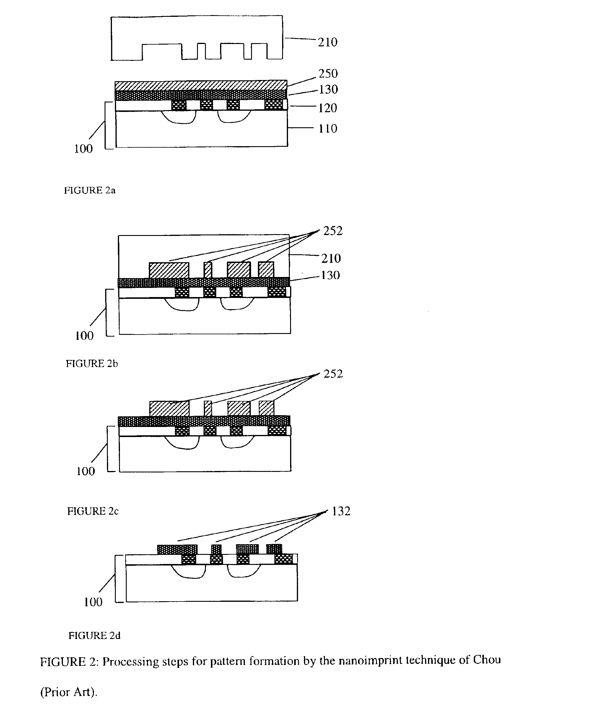
As indicated above, this represents a manufacturing technique for integrated devices using a dissolvable template that is low cost, and can be applied to nanoimprint techniques or to the pre-fabrication of portions of microdevices that are stored until their use is required. We now present a more detailed description of the best and preferred embodiments of the invention.

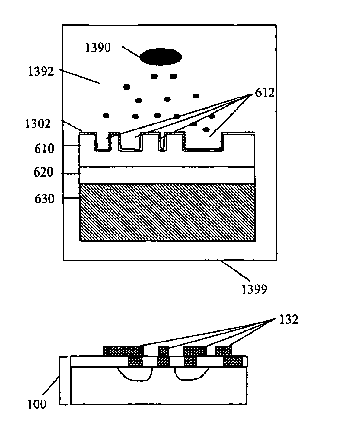
FIG. 5 shows a flowchart for a manufacturing process using this technique. Initially, as shown in FIG. 5a, step 500 creates a master pattern defining the layout of the structures to be fabricated. Step 510 represents the replication of the master in a template. Step 520 represents the transfer of the template to a carrier. In step 530, optional additional processing steps are carried out on the template. This is also the step where entire nanostructures or portions of other devices can be fabricated on the template. In step 540, the carrier and template, along with any structures fabricated on the template, are plac...


PUM

PropertyMeasurementUnit
widthaaaaaaaaaa
sizesaaaaaaaaaa
thicknessaaaaaaaaaa

Abstract

A method for the duplication of microscopic patterns from a master to a substrate is disclosed, in which a replica of a topographic structure on a master is formed and transferred when needed onto a receiving substrate using one of a variety of printing or imprint techniques, and then dissolved. Additional processing steps can also be carried out using the replica before transfer, including the formation of nanostructures, microdevices, or portions thereof. These structures are then also transferred onto the substrate when the replica is transferred, and remain on the substrate when the replica is dissolved. This is a technique that can be applied as a complementary process or a replacement for various lithographic processing steps in the fabrication of integrated circuits and other microdevices.

Description

FIELD OF THE INVENTIONThis invention relates to a new process for the replication of surface relief at the micrometer and the nanometer dimension scale. Furthermore, the process provides for the transfer of the replicated pattern from a master substrate to a second substrate. This invention describes a method of transfer lithography in which a disposable intermediate template is used. The process is also suitable for replicating and / or transferring single or multiple layers of microscopic elements that are to be used for photonic applications, metrology applications, and in the fabrication of integrated circuits and other microdevices.BACKGROUND OF THE INVENTIONMicrolithographic patterning of integrated circuits has made great improvements in the recent years. Prototype devices with dimensions less than 100 nm in width have been demonstrated, and are expected to enter routine production soon.These integrated devices are typically assembled sequentially, through a series of process s...

Claims


Application Information

Patent Timeline
Patent Type & Authority Patents(United States)
IPC IPC(8): G03F7/09B81C1/00B82B3/00G03F7/00H01L21/027
CPCB29C33/52B81C1/0046B82Y10/00G03F7/0002G03F7/091B82Y40/00Y10S438/942
Inventor SCHAPER, CHARLES DANIEL
Owner THE BOARD OF TRUSTEES OF THE LELAND STANFORD JUNIOR UNIV
Why Eureka
Try Eureka