Method of depositing a low k dielectric barrier film for copper damascene application
- Summary
- Abstract
- Description
- Claims
- Application Information
AI Technical Summary
Benefits of technology
Problems solved by technology
Method used
Image
Examples
Embodiment Construction
t to be considered limiting of its scope, for the invention may admit to other equally effective embodiments.
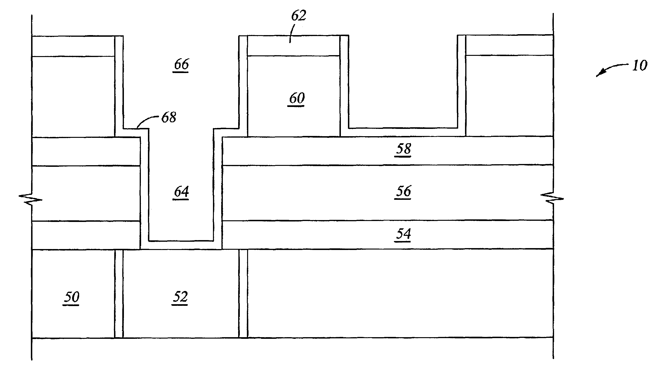
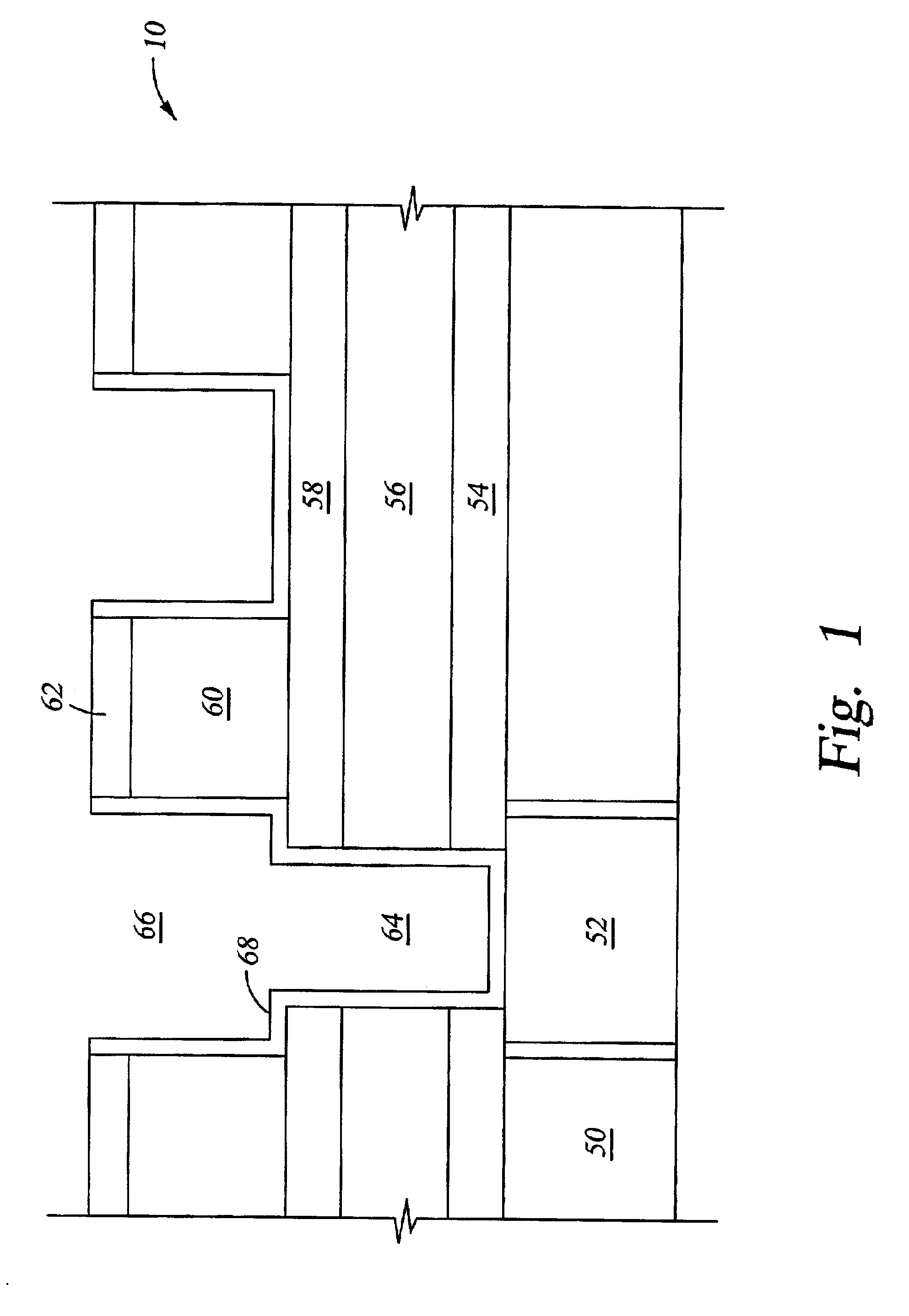
[0016]FIG. 1 is a schematic of a damascene structure using the low k dielectric film of the present invention as a barrier layer, an etch stop, and as an antireflective coating or a hard mask.
DETAILED DESCRIPTION OF THE PREFERRED EMBODIMENT
[0017]In one aspect, the invention provides a low k dielectric film and a method for making a low k dielectric film. The low k dielectric film is formed by reacting a gas mixture including a silicon source, a carbon source, and a nitrogen source which has the formula NR1R2R3. The silicon source and the carbon source may be separate compounds or an organosilicon compound. In one embodiment, the organosilicon compound may have the general formula SixCyHz, where x has a range from 1 to 2, y has a range from 1 to 6, and z has a range from 4 to 18. For example, methylsilane (SiCH6), dimethylsilane (SiC2H8), trimethylsilane (SiC3H10), tetramethyl...
PUM
| Property | Measurement | Unit |
|---|---|---|
| Temperature | aaaaa | aaaaa |
| Temperature | aaaaa | aaaaa |
| Pressure | aaaaa | aaaaa |
Abstract
Description
Claims
Application Information

