Selective base etching
- Summary
- Abstract
- Description
- Claims
- Application Information
AI Technical Summary
Benefits of technology
Problems solved by technology
Method used
Image


Examples
Embodiment Construction
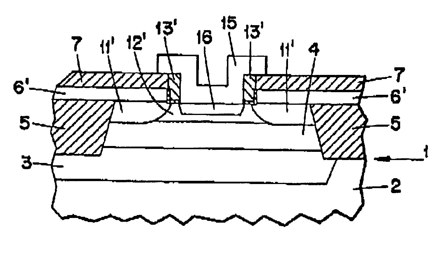
Shown in FIG. 1 is a silicon substrate 1, wherein the silicon may be monocrystalline, polycrystalline or microcrystalline but is preferably monocrystalline. As in FIG. 1 the substrate 1 may have various defined regions 2-5, which will be described below more in detail. Such regions may include a doped region, particularly a region doped with boron, and / or a region containing germanium. The substrate may alternatively be homogeneous. Any surface oxide present on the substrate 1, possibly having a thickness of some nanometers, can be removed by conveniently dipping the substrate in an HF bath or in an HF vapor.
In accordance with the invention there is deposited a layer 6 of silicon-germanium on the substrate 1 to a thickness of some hundreds of nanometers, preferably by employing RP-CVD technique typically in a temperature interval of 500-550 C. The exact temperature to achieve the desired layer structure will depend on the germanium concentration and level of in-situ doping of dopant...
PUM
 Abstract
Description
Claims
Application Information