Magnetoresistance effect element

a technology of magnetic coupling and effect element, applied in the field of magnetic resistance effect element, can solve the problems of weakened magnetic coupling via the nol, difficult to insert a nol into a pinned layer to maintain a high specular rate, and not so good specular ra

Inactive Publication Date: 2005-02-08
KK TOSHIBA
View PDF13 Cites 67 Cited by
  • Summary
  • Abstract
  • Description
  • Claims
  • Application Information

AI Technical Summary

Benefits of technology

[0081]These magnetoresistance effect element may be effectively a bottom type SV wherein an antiferromagnetic film is formed below a pinned layer, or a top type SV wherein an antiferromagnetic film is formed above a pinned layer.
[0082]The above described magnetoresistance effect element can be used as a magnetic head for reading recording data out of a med

Problems solved by technology

However, it is very difficult to insert a NOL into a pinned layer to maintain a high specular rate while holding a magnetically sufficient strong coupling of top and bottom pinned layers via the NOL.
For example, when oxygen gas is caused to flow to form a NOL, if the oxygen exposure amount is increased at an oxidizing step of forming the NOL in order to obtain a high specular rate, there is a problem in that the magnetic coupling via the NOL is weakened whereas the specular rate is not so improved.
Inversely, if oxidation is carried out at a weak oxygen exposure amount, there is a problem in that the magnetic coupling of the top and bottom pinned layers via the NOL increases whereas a high specular rate is not obtained and the rate of change in MR is not so improved.
However, since no energy is applied in the oxidizing process, the control range of physical properties of a NOL capable of being formed is narrow, and the control range in the process is also very narrow.
However, since the surface of a sample is exposed to suspended oxygen before oxygen plasma is fired (produced), there is a problem in that an oxide film is formed by simple oxygen gas, so that the same layer as a natural oxide film is formed in the portion of an initially grown NOL.
Although it is possible to carry out a high energy oxidation by plasma energy, there is a problem in t

Method used


Image

  • Magnetoresistance effect element
  • Magnetoresistance effect element
  • Magnetoresistance effect element

Examples


example 1

[0294]Examples of the eighth embodiment of the present invention will be described below.

[0295]An SV film having the following construction was prepared by the sputtering method, and MR characteristics were compared.

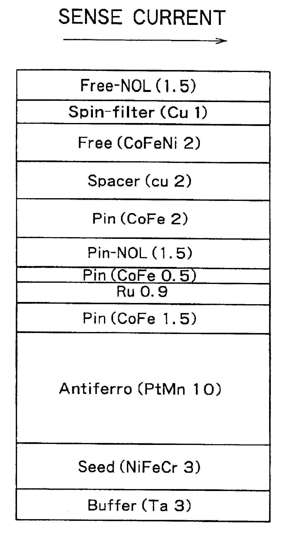
[0296]Ta 3 nm (Underlying Layer) / NiFeCr 3 nm (Underlying Layer / PtMn 10 nm (Antiferromagnetic Layer) / CoFe 1.5 nm (Pinned layer) / Ru 0.9 nm (Pinned layer) / CoFe 0.5 nm (Pinned layer) / Fe Oxide 1.5 nm (Electron Reflective Layer) / CoFe 2 nm (Pinned layer) / Cu 2 nm (Non-magnetic Intermediate Layer) / CoFe 2 nm (Free Layer) / Cu 1 nm (High Conductive Layer) / X (Electron Reflective Layer) / Amorphous Alumina 100 nm

[0297]In this SV film, an oxidizing process was carried out by various oxidizing methods to form an Fe oxide or Cr oxide having a thickness of 1 nm as the electron reflective layer X to observe the kind and abundance ratio of the product by the extended X-ray absorption fine structure (EXAFS) and crystalline properties by the cross-section TEM. The results thereof are shown below...


PUM


Abstract

There are provided a magnetoresistance effect element, a magnetic head, a magnetic head assembly and a magnetic recording system, which have high sensitivity and high reliability. The magnetoresistance effect element has two ferromagnetic layers, a non-magnetic layer provided between the ferromagnetic layers, and a layer containing an oxide or nitride as a principal component, wherein the layer containing the oxide or nitride as the principal component contains a magnetic transition metal element which does not bond to oxygen and nitrogen and which is at least one of Co, Fe and Ni.

Description

CROSS REFERENCE TO RELATED APPLICATION[0002]This application is based upon and claims benefit of priority from the prior Japanese Patent Applications No. 2000-268934, filed on Sep. 5, 2000; and No. 2000-269099, filed on Sep. 5, 2000; the contents of which are incorporated herein by reference.BACKGROUND OF THE INVENTION[0003]1. Field of the Invention[0004]The present invention relates generally to a magnetoresistance effect element, a method and system for fabricating the same, and a magnetic reading system using the same. More specifically, the invention relates to a magnetoresistance effect element using a spin-valve film having an oxide layer or a nitride layer as a magnetoresistance effect improving layer for causing a specular reflection of electrons, a method and system for fabricating the same, and a magnetic reading system using the same.[0005]2. Description of Related Art[0006]In order to realize the enhancement of the density of hard disk drives (HDDs), a giant magnetoresis...

Claims


Application Information

Patent Timeline
IPC IPC(8): H01F10/00H01F10/32G11B5/39
CPCB82Y10/00B82Y25/00H01F10/3272H01L43/10H01F10/3259H01L43/08G11B5/3903G11B2005/3996H01F41/325Y10T428/1121Y10T428/1114H01F10/3295G11B5/3932H10N50/85H10N50/10
Inventor FUKUZAWA, HIDEAKIKOI, KATSUHIKOFUKE, HIROMITOMITA, HIROSHIIWASAKI, HITOSHISAHASHI, MASASHI
Owner KK TOSHIBA
Why Eureka
Try Eureka