

Components for vacuum deposition apparatus and vacuum deposition apparatus therewith, and target apparatus
- Summary
- Abstract
- Description
- Claims
- Application Information
AI Technical Summary
Benefits of technology
Problems solved by technology
Method used
Image

Examples
embodiment 1
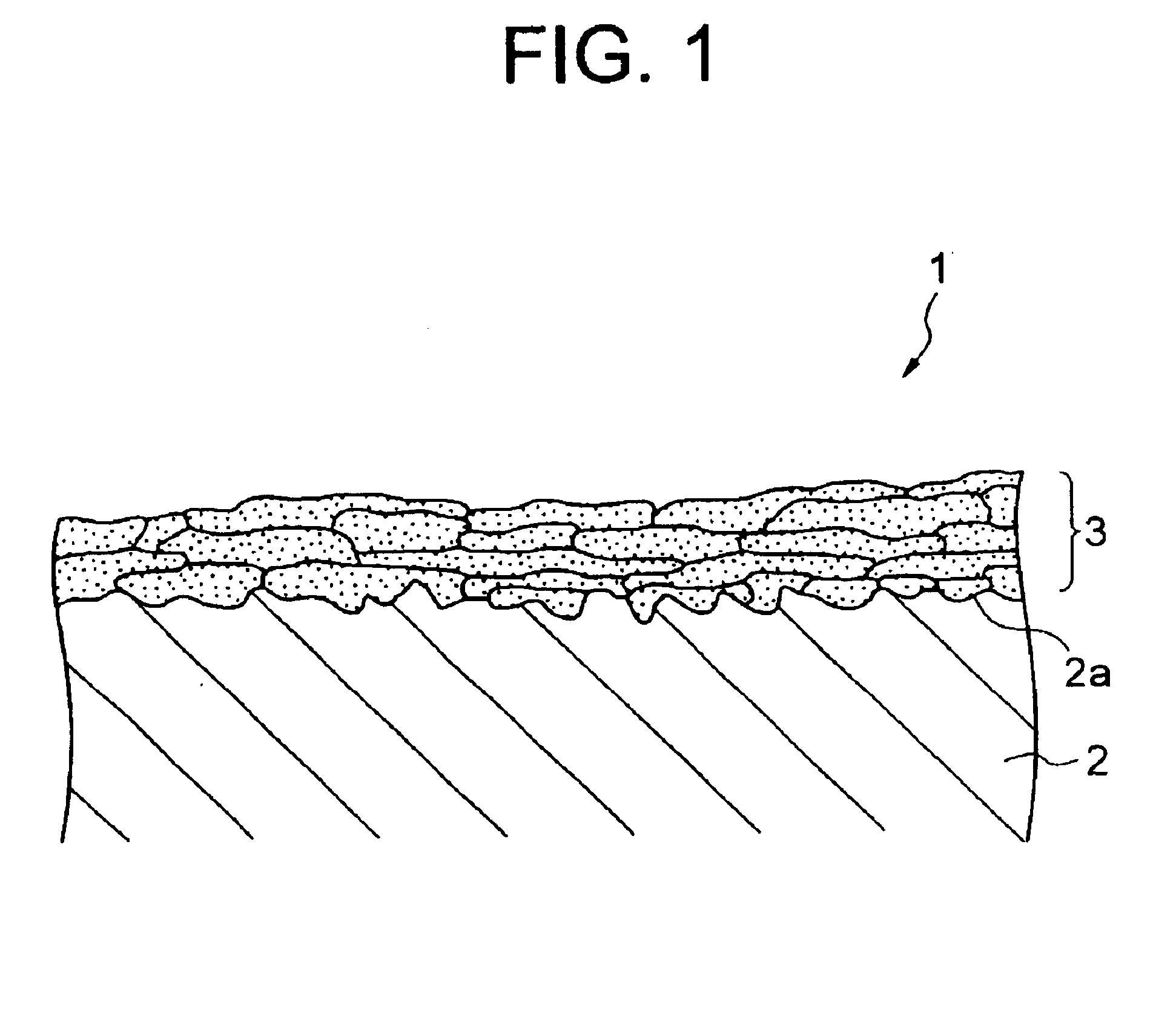
As obvious from FIG. 8, in the magnetron sputtering apparatus due to Embodiment 1, the amount of the generated particles is low with stability up to 150 lots. On the other hand, in the magnetron sputtering apparatus according to Comparative Example 1, it is found that in addition to there being sporadic particle generation, overall amount of the generated particles is larger. From these, it is found that by the use of the spray deposit according to Embodiment 1, the particles may be effectively and stably suppressed from generating.
embodiment 7
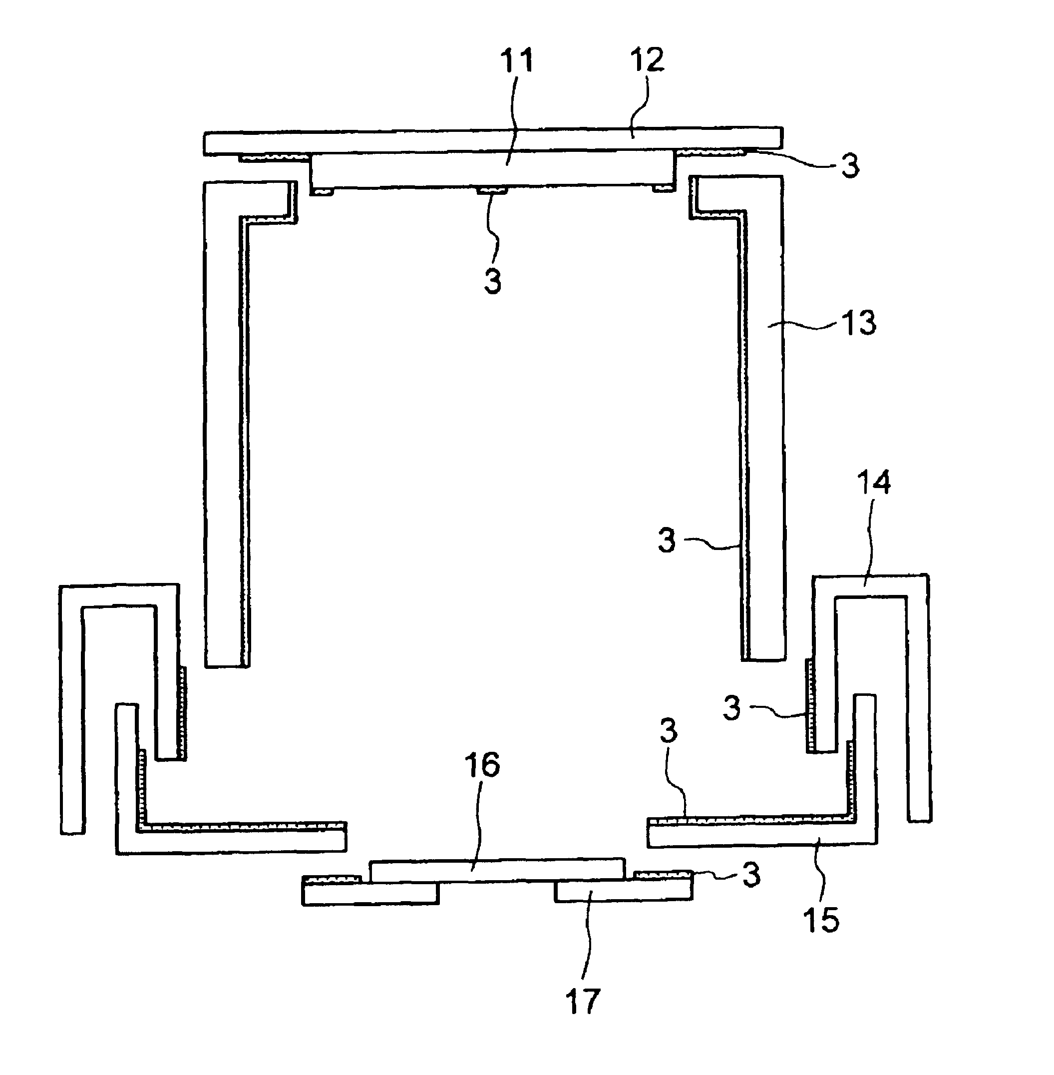
To the components (SUS304 substrate) each of the earth shield 13, the upper deposition preventive plate 14, the lower deposition preventive plate 15 and the platen ring 17 of the sputtering apparatus shown in FIG. 7, spray deposits each shown in Table 7 are coated by means of the plasma spraying. Then, the surface of the spray deposits each, after cleansing, is heat treated under the conditions shown in Table 7. The surface roughness and hardness of each spray deposit are shown in Table 7.
The conditions of coating (conditions for plasma spraying) of the spray deposits each are, for Al, a particle diameter of powder raw material from 45 to 90 μm, an electric current 500 A, a voltage 75 V, an Ar flow rate 73 L / min and a H2 flow rate 8 L / min; for Cu, a particle diameter of powder raw material from 30 to 90 μm, an electric current 500 A, a voltage 65 V, an Ar flow rate 73 L / min and a H2 flow rate 5 L / min; for W, a particle diameter of powder raw material of 45 μm or less, an electric cu...
embodiment 8
To the components each of the earth shield 13, the upper deposition preventive plate 14, the lower deposition preventive plate 15 and the platen ring 17 of the sputtering apparatus shown in FIG. 7, two-layered spray deposits each shown in Table 8 are coated, respectively. Then, the surface of the spray deposits each, after cleansing, is heat treated under the conditions shown in Table 8. The surface roughness and hardness of each spray deposit are shown in Table 8.
As the substrate, Al alloy is used for sample No. 5 in Table 8, other than this SUS 304 being used. The conditions for coating of the spray deposits each are fundamentally the same with Embodiment 7. The Al spray deposit of sample No. 3 in Table 8 is arc sprayed with an Al wire of a diameter of 1.6 mm as raw material for spraying and under the conditions of a current of 200 A and a voltage of 30 V.
Next, the components each are assembled in the magnetron sputtering apparatus, on 8-inch wafers, thin films shown in Table 8 ar...
PUM
| Property | Measurement | Unit |
|---|---|---|
| Length | aaaaa | aaaaa |
| Length | aaaaa | aaaaa |
| Length | aaaaa | aaaaa |
Abstract
Description
Claims
Application Information