
Plating method and apparatus using contactless electrode

a contactless electrode and electrode technology, applied in the field of semiconductor processing, can solve the problems of deficiency in several ways of the electroplating process known in the art, variation in current density, potential drop between the wafer edge and the edge of the wafer edg

Inactive Publication Date: 2005-02-15
JAIRATH RAHUL
View PDF3 Cites 29 Cited by
  • Summary
  • Abstract
  • Description
  • Claims
  • Application Information

AI Technical Summary

Benefits of technology

In various other embodiments, spacers are utilized to separate a plurality of electrodes. The spacer may be made conductive so that it may operate as an anode as well. In other embodiments, power to the various electrodes are sep

Problems solved by technology

Electroplating processes known in the art are deficient in several ways.
First, thin seed layers tend to be resistive and result in a potential drop between the wafer edge where electrode contact has been established and the wafer center where there is no direct electrode contact.
The potential drop causes variations in current density across the wafer surface, which may contribute to poor plating uniformity.
Secondly, features with small dimensional sizes and / or high aspect ratios are often plated with voids in the features and residual topography on the plated metal surface.
Thirdly, a large amount of metal may need to be plated for the plating process to be integrated with subsequent processes such as polishing.
Since large amounts of metal are first plated and subsequently polished away, the plating and polishing processes represented as an integrated module may be inefficient and costly.
However, metal fillers may damage the wafer surface as the wafer rotates with respect to the sponge, thereby resulting in poor device yields.
Furthermore, conducting polymers, such as polyaniline, lack the structural integrity to withstand the stress caused by rotating the wafer with respect to the sponge.
However, pushing such contacts against the wafer surface may damage the plated metal and underlying layers, particularly due to sliding friction when the wafer is rotated with respect to the contacts.
Furthermore, such wafer surface damage may result in poor device yields.
However, the electrolyte layer is conductive and provides a direct path of current flow between the electrical contacts and the anode that may result in poor power and plating efficiency.
This technique reduces void formation and local topography within specific regions of the semiconductor device, but generally does not benefit topography globally across the semiconductor device.
Polishing occurs in high regions that are not masked, increasing planarity of the semiconductor device.
However, this technique generally requires two discrete processes and is costly to implement.
Another disadvantage of this technique is that the masks utilized are often degraded by the electrolyte itself and may result in poor planarity.
However, the polishing action is primarily an electropolishing action and is isotropic such that the resulting surface of the plated metal is locally planar but has poor global planarity.
Another disadvantage of this technique is that for plating to be practical, the net plating action may need to be substantially larger than the net polishing action, usually by arranging the bipolar electrode and wafer such that the portion of the wafer surface being plated is substantially larger than the portion being polished.
Since the net current flow between the anode and cathode is fixed, this arrangement may lead to current density differences between the two portions of the wafer surface and uneven plating across the wafer surface.
Still another disadvantage of this technique is that it increases the path through which current flows from the anode to the cathode.
Thus, the capacitance and resistance of the current path is increased making it less responsive to fluctuating currents, such as in pulse plating, and may result in poorly filled features on the wafer surface.
However, cross-contamination often occurs between the polishing and plating chambers, degrading the quality of the plated metal.
Generally, the use of multiple chambers increases complexity of the apparatus resulting in higher costs.
Yet another disadvantage of this technique is that obtaining sufficient planarity often requires use of hard pads pushed against the substrate surface with a high force, damaging the plated metal and underlying layers.
However, electroless plating rates are significantly slower compared to electro-plating and commercially less viable for many applications.
Another disadvantage of electroless plating is that it is a conformal deposition process and suffers from the planarization related disadvantages described above.
These techniques cannot be applied to electroless plating since electroless plating tools do not use anode and / or cathode electrodes.
Intermittently applying a pad to the wafer surface during electroless plating may improve planarization, but further reduces effective plating rate of the metal and impacts commercial viability.
Therefore, planarization in electroless plated surfaces still pose disadvantages.
In addition, electroless plating baths often use environmentally hazardous materials (such as formaldehyde, a known carcinogen) significantly limiting their use in commercial applications.
Yet another disadvantage of electroless plating is that since it does not depend on electric currents, it may be a difficult process to regulate.

Method used


Image

  • Plating method and apparatus using contactless electrode
  • Plating method and apparatus using contactless electrode
  • Plating method and apparatus using contactless electrode

Examples


Embodiment Construction

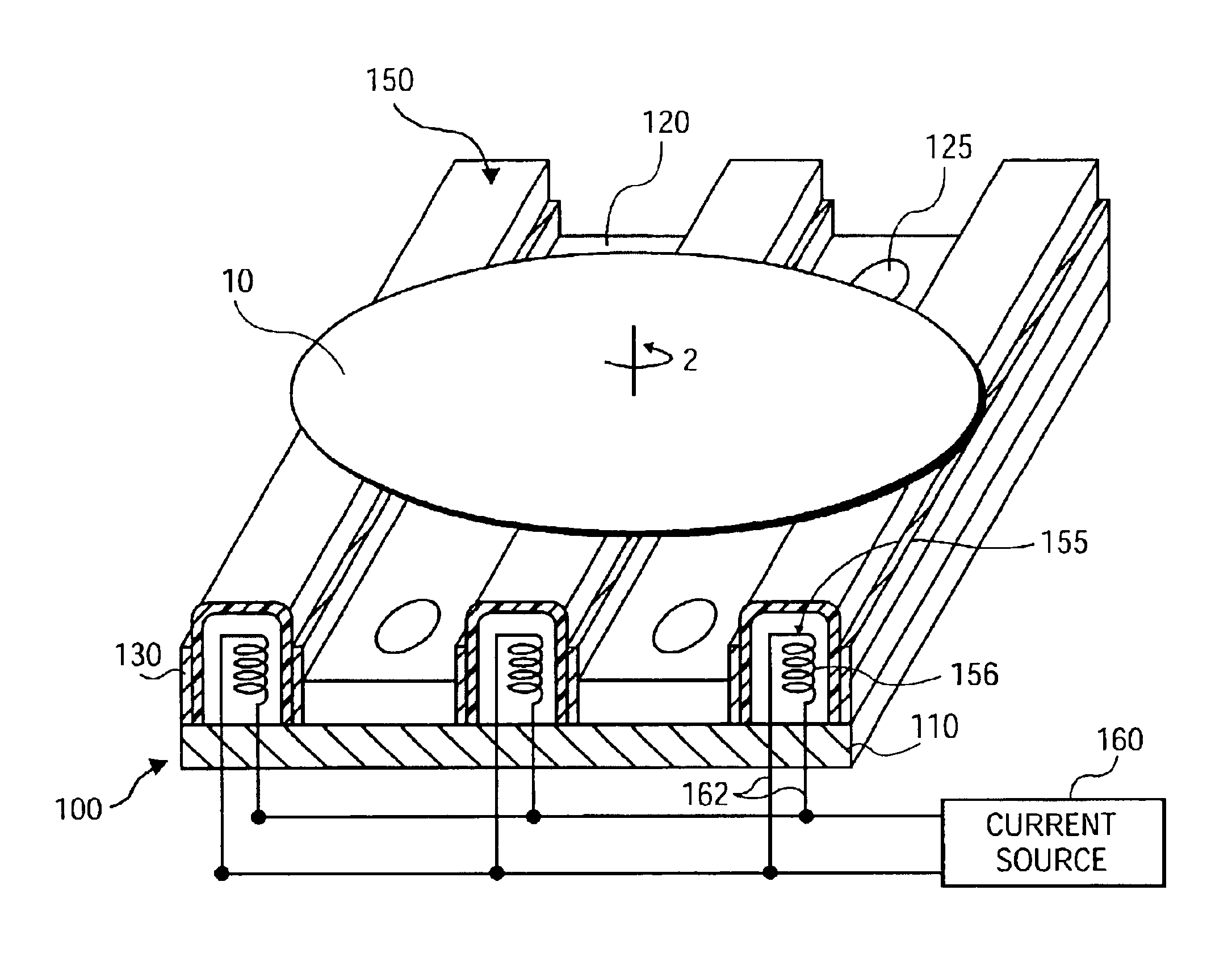
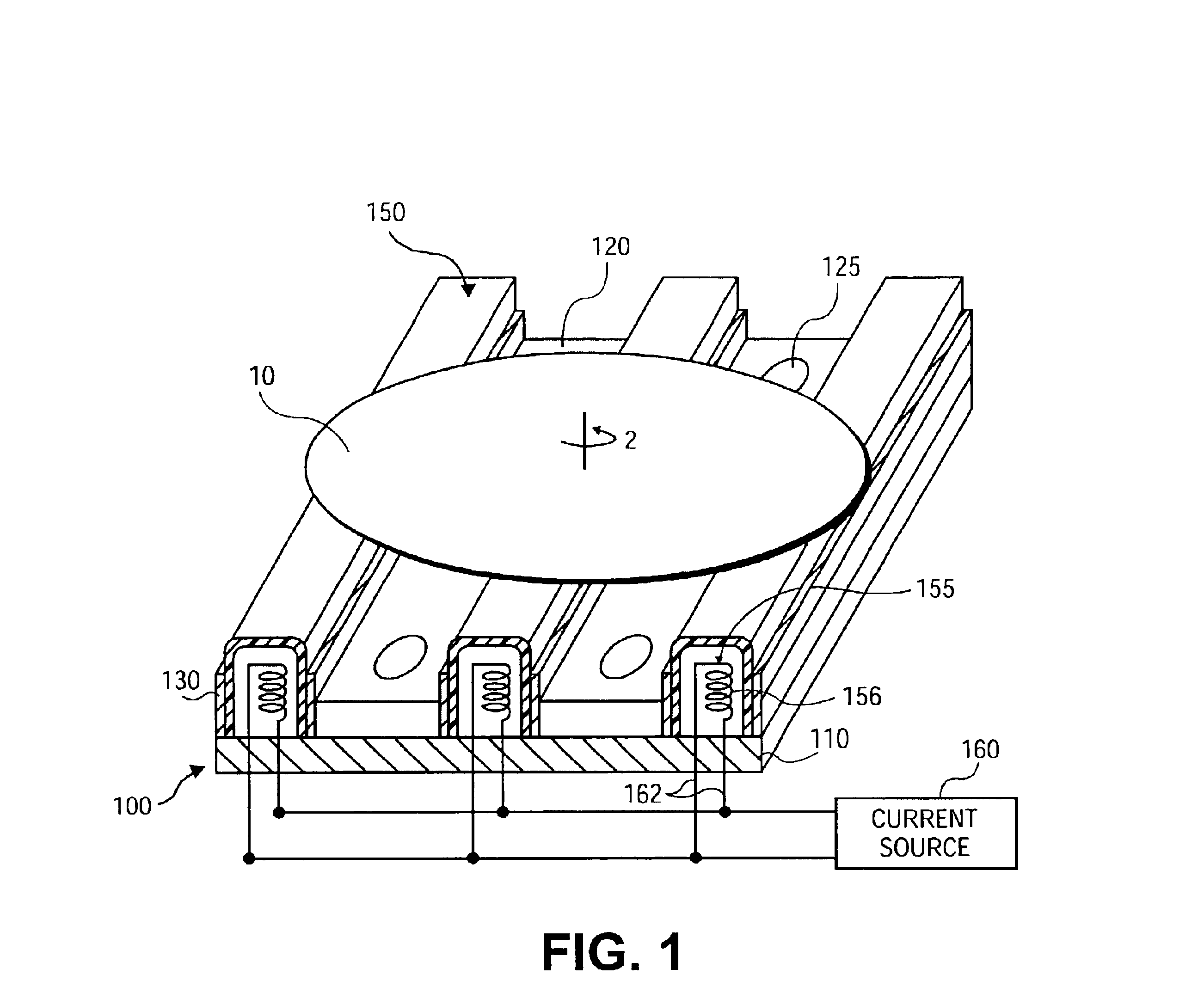
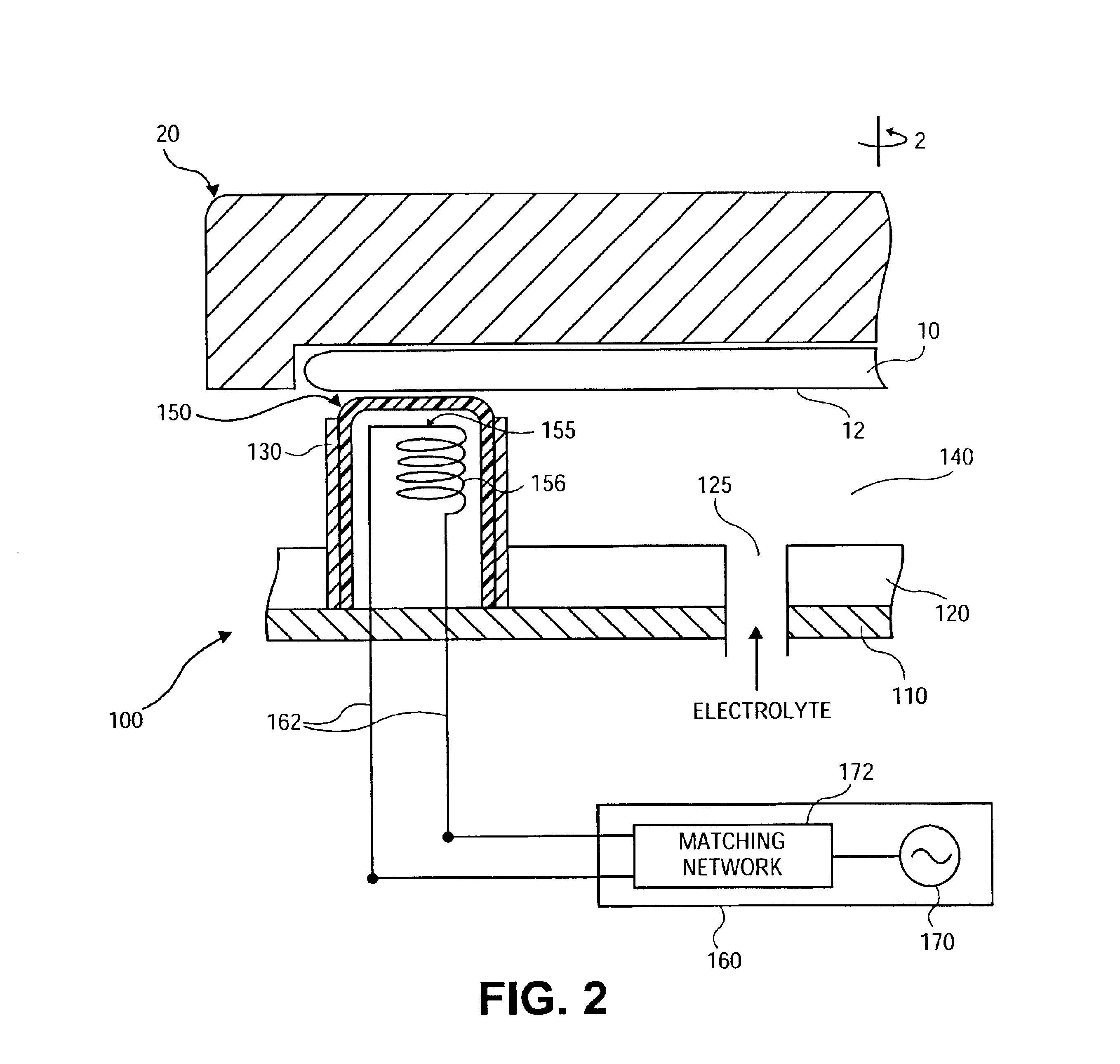
The described embodiments of the present invention address plating a metal (metal being defined herein to include not only the metal, but metal alloy and other compositions having metal that provide metal properties when deposited) layer on a wafer surface or a layer formed on a wafer, using a contactless electrode, having an inductive or capacitive element, to generate current and / or voltage on the wafer surface. Although a semiconductor wafer is used as an example to describe the embodiments herein, other substrates, including a flat panel or magnetic film head, may be used instead. Furthermore, while described embodiments refer to the plating of a metal, the described techniques may be employed to plate a metal, metal alloy, or other conductive materials or layers.

FIGS. 1 and 2 illustrate a perspective view and a cross-sectional detailed view, respectively, of one embodiment of the present invention. The embodiment is illustrated as assembly 100. A wafer carrier 20 supports a waf...


PUM

PropertyMeasurementUnit
Electric chargeaaaaaaaaaa
Currentaaaaaaaaaa
Electrical conductoraaaaaaaaaa

Abstract

A plating method and apparatus using contactless electrode is described. In one embodiment an inductive element is placed proximally to a substrate and a moving electromagnetic field generates an emf in the substrate to plate the surface. In another embodiment, a conductive plate is used, so that the conductive plate and the wafer, separated by a dielectric material, operate as two plates of a capacitor when voltage is applied to the conductive plate. The resulting electrostatic field impresses a charge potential on the substrate to plate the surface of the substrate.

Description

FIELD OF THE INVENTIONThis invention relates generally to semiconductor processing and, more specifically, to a method and apparatus for plating metals on a semiconductor wafer.BACKGROUND OF THE INVENTIONPlating metals by electroplating or electroless plating over a seed layer on a wafer is a common process in the manufacture of semiconductor devices. Requirements for plating processes in semiconductor device manufacturing have become increasingly stringent as device features become smaller and wafer sizes become larger.One such property is uniform plating across the wafer surface. Another desirable property is to uniformly fill device features (such as vias and trenches) such that no voids exist in the features and the surface of the plated metal is globally planar. Yet another property is to plate metal without damaging the plated metal or any underlying layer. Still another property is for the plating process to be cost effective.Electro-plating typically involves a rotating wafe...

Claims


Application Information

Patent Timeline
IPC IPC(8): C25D17/00C25D5/00C25D5/18C25D7/12C25D17/06C25D17/10
CPCC25D5/18C25D17/001C25D17/10C25D17/06
Inventor JAIRATH, RAHUL
Owner JAIRATH RAHUL
Features
  • Generate Ideas
  • Intellectual Property
  • Life Sciences
  • Materials
  • Tech Scout
  • Unparalleled Data Quality
  • Higher Quality Content
  • 60% Fewer Hallucinations
Learn More