
Process for forming a low dielectric constant fluorine and carbon-containing silicon oxide dielectric material

a technology of fluorine and carbon-containing silicon oxide, which is applied in the field of integrated circuit structures, can solve the problems of reducing the capacitance of the dielectric material, destroying the incorporated hydrocarbons, and losing speed and increasing cross-talk

Inactive Publication Date: 2005-02-22
BELL SEMICON LLC
View PDF61 Cites 18 Cited by
  • Summary
  • Abstract
  • Description
  • Claims
  • Application Information

AI Technical Summary

Benefits of technology

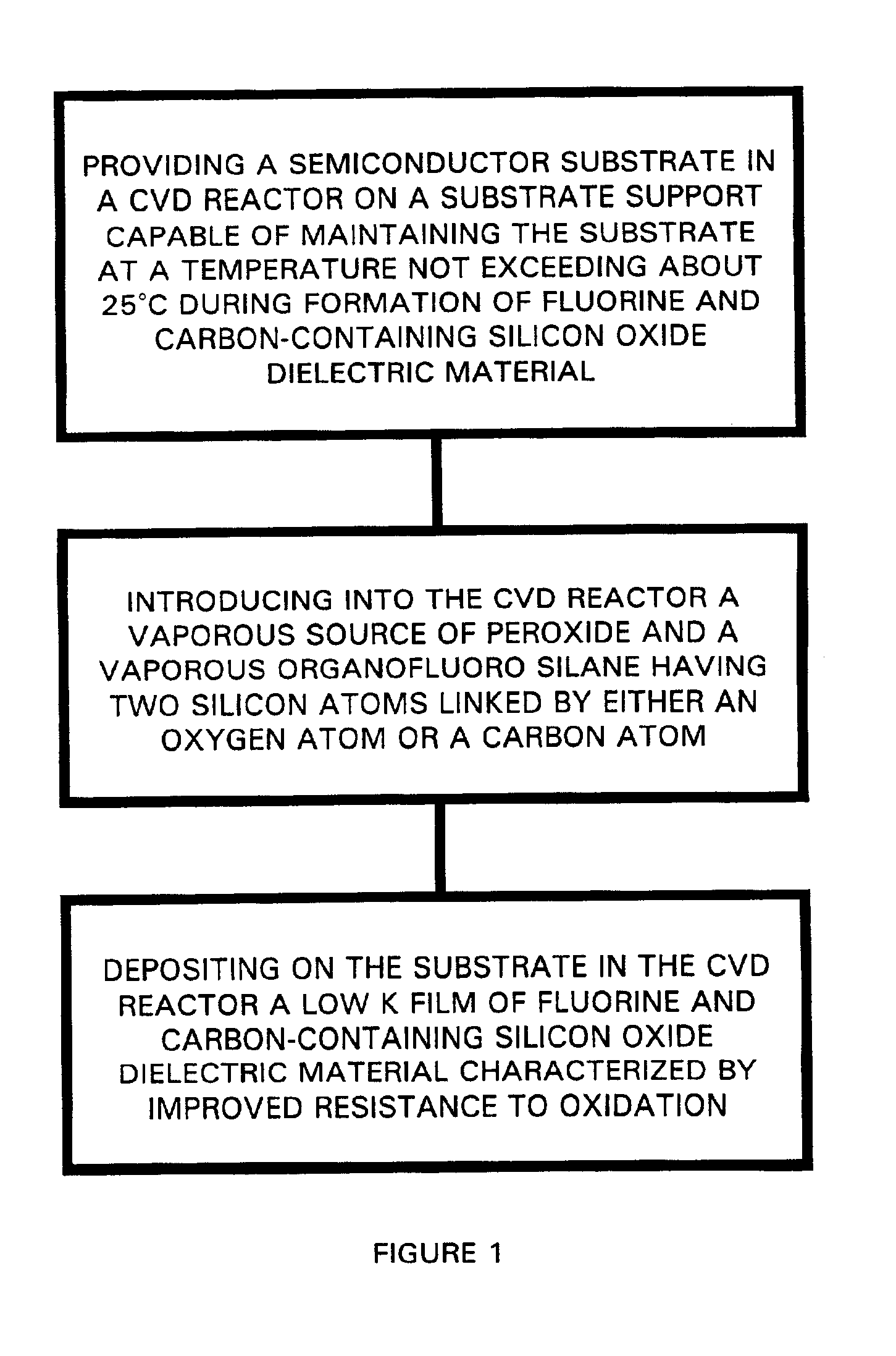
The invention provides a process for forming a low k fluorine and carbon-containing silicon oxide dielectric material by reacting with an oxidizing agent one or more silanes that include one or more organofluoro silanes selected from: (a) an organofluoro silane containing two silicon atoms linked by one oxygen atom; (b) an organofluoro silane containing two silicon atoms linked by one or more carbon atoms, where the one or more carbon atoms each are bonded to one or more fluorine atoms, or to one or more organofluoro moieties, or to a combination thereof; and (c) an organofluoro silane containing a silicon atom bonded to an oxygen atom. In one embodiment, the process of the invention is carried out using one or more organofluoro silanes having the formula: (CxF2x+1)(R1)(R2)Si((L)Si(R3)(R4))n(R5) where x=1 to 5; n=1 to 5; each of the n L's is selected from O and (C(R6)2)m; m=1 to 4; R1 and R2 are selected from the same or different leaving group and the same or different (CxF2x+1); each of the n R3's and n R4's is independently selected from the same or different leaving group and the same or different (CxF2x+1); R5 is a leaving group; and each of the 2n*m or fewer R6's is independently selected from F and the same or different (CxF2x+1).
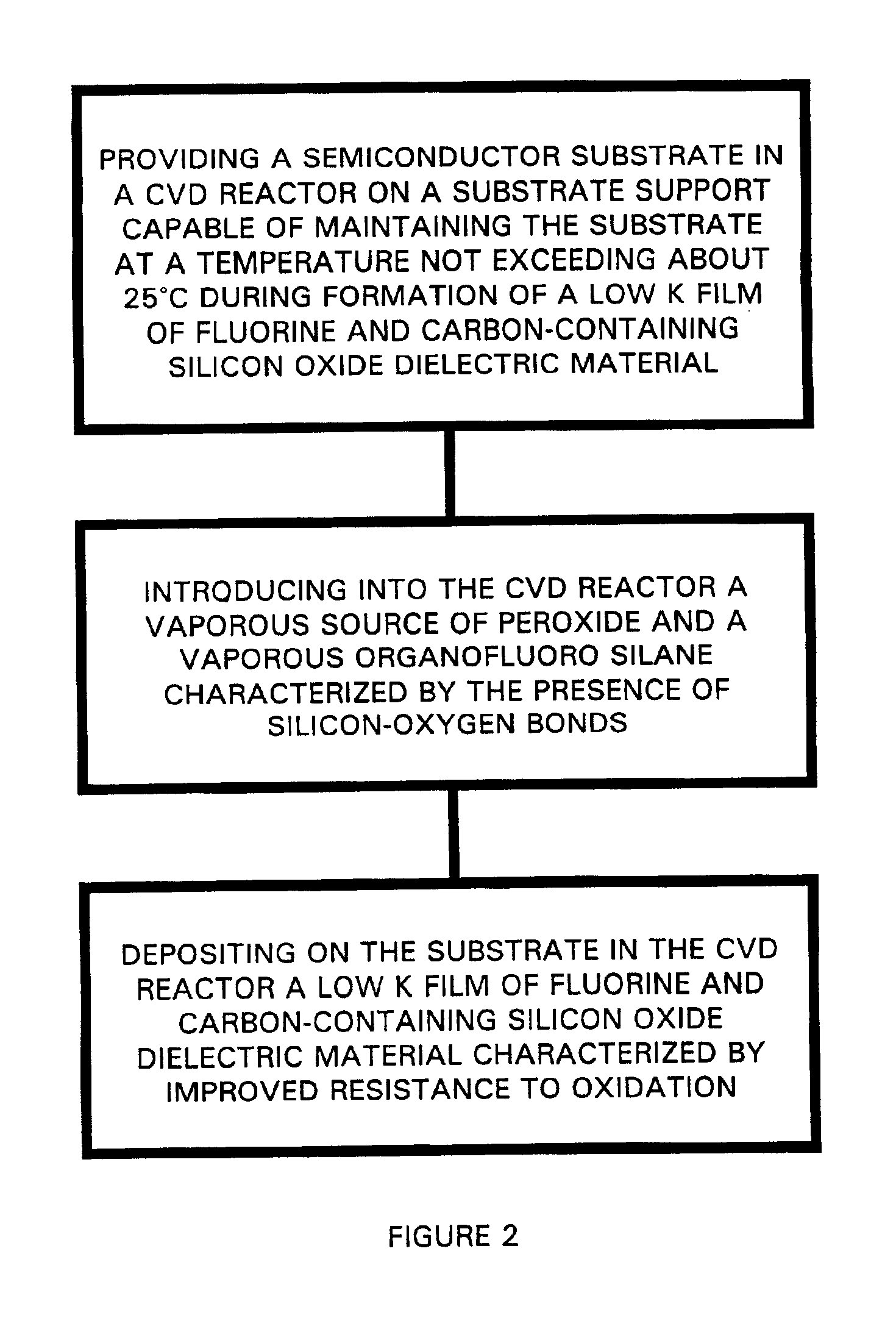
The invention also provides a process for forming a low k fluorine and carbon-cont

Problems solved by technology

As a result, capacitance has increased between such conductive portions, resulting in loss of speed and increased cross-talk.
While such carbon-doped silicon oxide dielectric materials do exhibit the desired low k (i.e., dielectric constants below about 3.0), resulting in reduced capacitance of the dielectric material, a major problem of such carbon-doped silicon oxide is a low resistance to oxidation during subsequent processing steps that results in a destruction of the incorporated hydrocarbons and a resulting increase in the overall dielectric constant of the dielectric material.
However, the precursor compound used by Sugahara yielded only approximately 15% CF3 content in the product dielectric layer.
Further, it is known that dielectric films produced by high temperature ozone processes are characterized by poor gap-fill, while continuous shrinkage in feature size of integrated circuit structure demands an increased gap-fill capability.

Method used


Image

  • Process for forming a low dielectric constant fluorine and carbon-containing silicon oxide dielectric material
  • Process for forming a low dielectric constant fluorine and carbon-containing silicon oxide dielectric material
  • Process for forming a low dielectric constant fluorine and carbon-containing silicon oxide dielectric material

Examples


example 1

The following example demonstrates the process of the invention in the formation of a low k fluorine and carbon-containing silicon oxide dielectric material at low temperature using the mild oxidizing agent, hydrogen peroxide.

Di-trifluoromethyl-disiloxane (CF3)H2SiOSiH2(CF3) and hydrogen peroxide can be introduced into a reaction chamber containing a cooled substrate support therein on which is mounted a silicon substrate on which the reaction product will deposit. The reaction chamber is advantageously maintained at a pressure of about 1-5 Torr. Both the di-trifluoromethyl-disiloxane and the hydrogen peroxide are introduced into the chamber in a gaseous or vaporous phase. The delivery system for the reactants is maintained at about 100° C., which ensures delivery of the reactants into the chamber as gases or vapors. Flow rates of the individual reactants will depend upon chamber size and will also vary with the particular reactants. During the reaction and deposition, the temperatu...

example 2

The following example demonstrates the process of the invention in the formation of a low k fluorine and carbon-containing silicon oxide dielectric material using the strong oxidizing agent, ozone.

Di-trifluoromethyl-tetramethyl-disiloxane (CF3)(CH3)2SiOSi(CH3)2CF3 and ozone can be introduced into a reaction chamber containing a silicon substrate on which the reaction product will deposit. The reaction chamber is advantageously maintained at a pressure of about 760 Torr. Both the di-trifluoromethyl-tetramethyl-disiloxane and the ozone are introduced into the chamber in a gaseous or vaporous phase. Flow rates of the individual reactants will depend upon chamber size and will also vary with the particular reactants. During the reaction and deposition, the temperature of the substrate support in the reaction chamber is maintained at a temperature of about 350° C. The reaction and deposition is carried out for a period of time sufficient to form the layer of low k fluorine and carbon-con...


PUM

PropertyMeasurementUnit
Dielectric constantaaaaaaaaaa

Abstract

The invention provides a process for forming a low k fluorine and carbon-containing silicon oxide dielectric material by reacting with an oxidizing agent one or more silanes that include one or more organofluoro silanes selected from: (a) an organofluoro silane containing two silicon atoms linked by one oxygen atom; (b) an organofluoro silane containing two silicon atoms linked by one or more carbon atoms, where the one or more carbon atoms each are bonded to one or more fluorine atoms, or to one or more organofluoro moieties, or to a combination thereof; and (c) an organofluoro silane containing a silicon atom bonded to an oxygen atom. The invention also provides a process for forming a low k fluorine and carbon-containing silicon oxide dielectric material by reacting with an oxidizing agent one or more silanes that include one or more organofluoro silanes characterized by the presence of Si—O bonds.

Description

BACKGROUND OF THE INVENTION1. Field of the InventionThis invention relates to integrated circuit structures. More particularly this invention relates to the formation of a low dielectric constant (k) fluorine and carbon-containing silicon oxide dielectric material for use in the formation of integrated circuit structures.2. Description of the Related ArtThe shrinking of integrated circuits has resulted in levels of electrically conductive interconnects being placed closer together vertically, as well as reduction of the horizontal spacing between the electrically conductive interconnects, such as metal lines, on any particular level of such interconnects. As a result, capacitance has increased between such conductive portions, resulting in loss of speed and increased cross-talk. One proposed approach to solving this problem of high capacitance is to replace the conventional silicon oxide (SiO2) dielectric material, having a dielectric constant (k) of about 4.0, with another insulati...

Claims


Application Information

Patent Timeline
IPC IPC(8): C23C16/40
CPCC23C16/401Y10T428/30
Inventor ARONOWITZ, SHELDONZUBKOV, VLADIMIR
Owner BELL SEMICON LLC
Learn More