Half-bridge high voltage gate driver providing protection of a transistor

Active Publication Date: 2005-02-22
INFINEON TECH AMERICAS
View PDF1 Cites 38 Cited by
  • Summary
  • Abstract
  • Description
  • Claims
  • Application Information

AI Technical Summary

Benefits of technology

A gate driver integrated circuit for switching one or more power transistors uses an external supply voltage and an external controller. The integrated circuit comprises an output stage for each of the power transistors, an input stage and a fault control circuit integrated in the integrated circuit. In operation, the output stage is coupled to the power transistor, such that a desaturation state of the power transistor may be detec

Problems solved by technology

Generally, there are two parasitic capacitances between the gate to source and the gate to drain that may cause switching delays if the gate driver does n

Method used


Image

  • Half-bridge high voltage gate driver providing protection of a transistor
  • Half-bridge high voltage gate driver providing protection of a transistor
  • Half-bridge high voltage gate driver providing protection of a transistor

Examples


Embodiment Construction

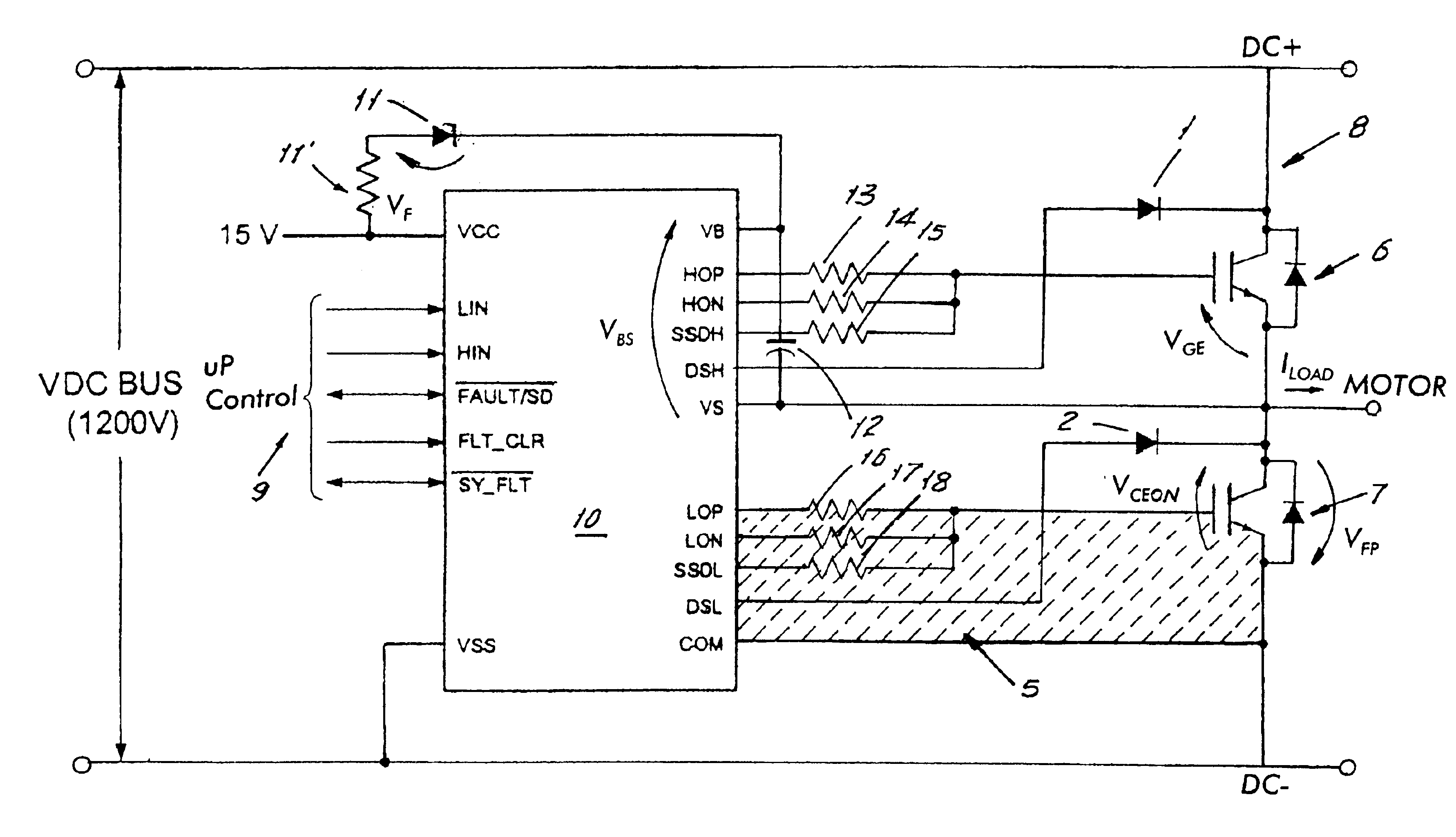
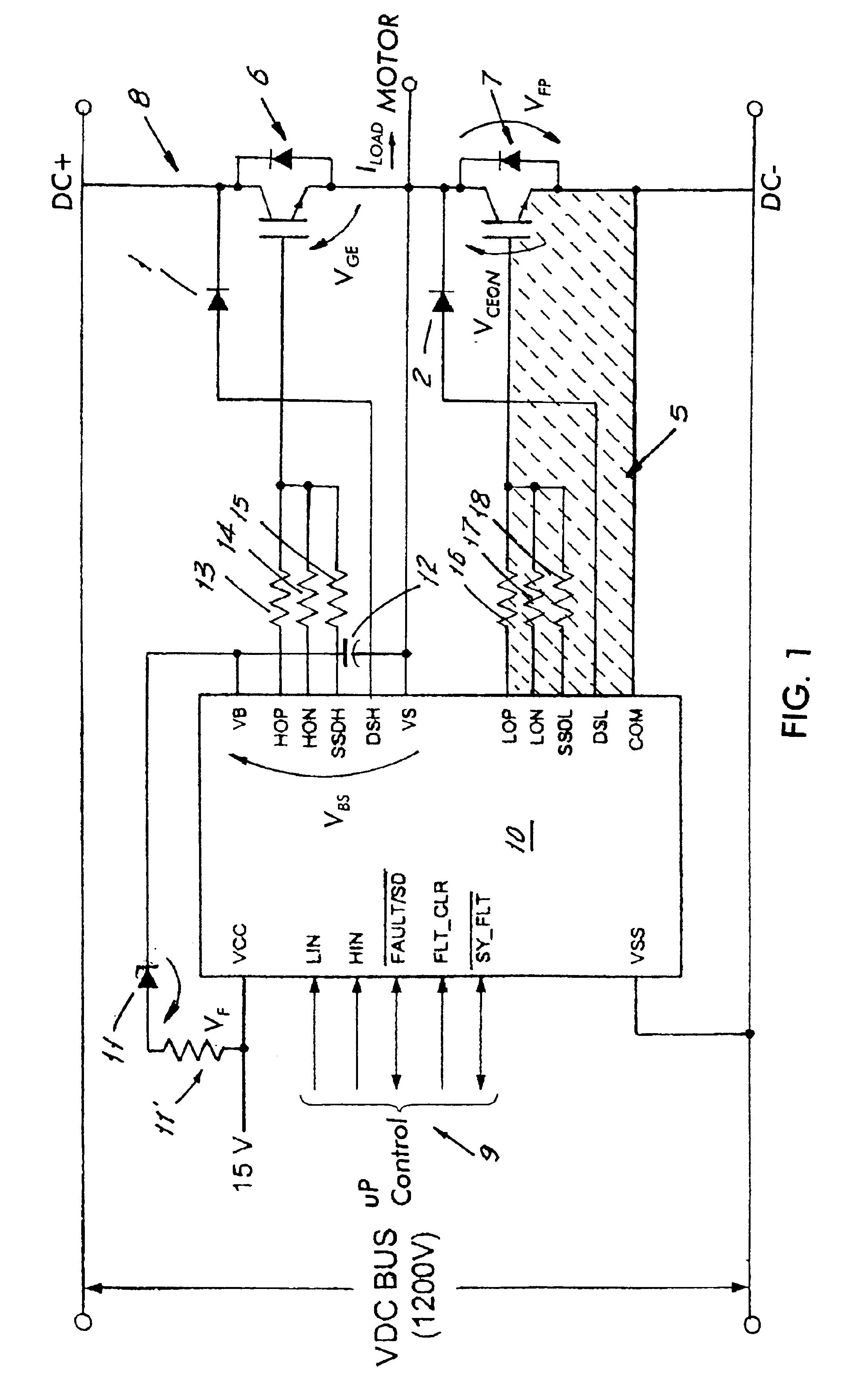
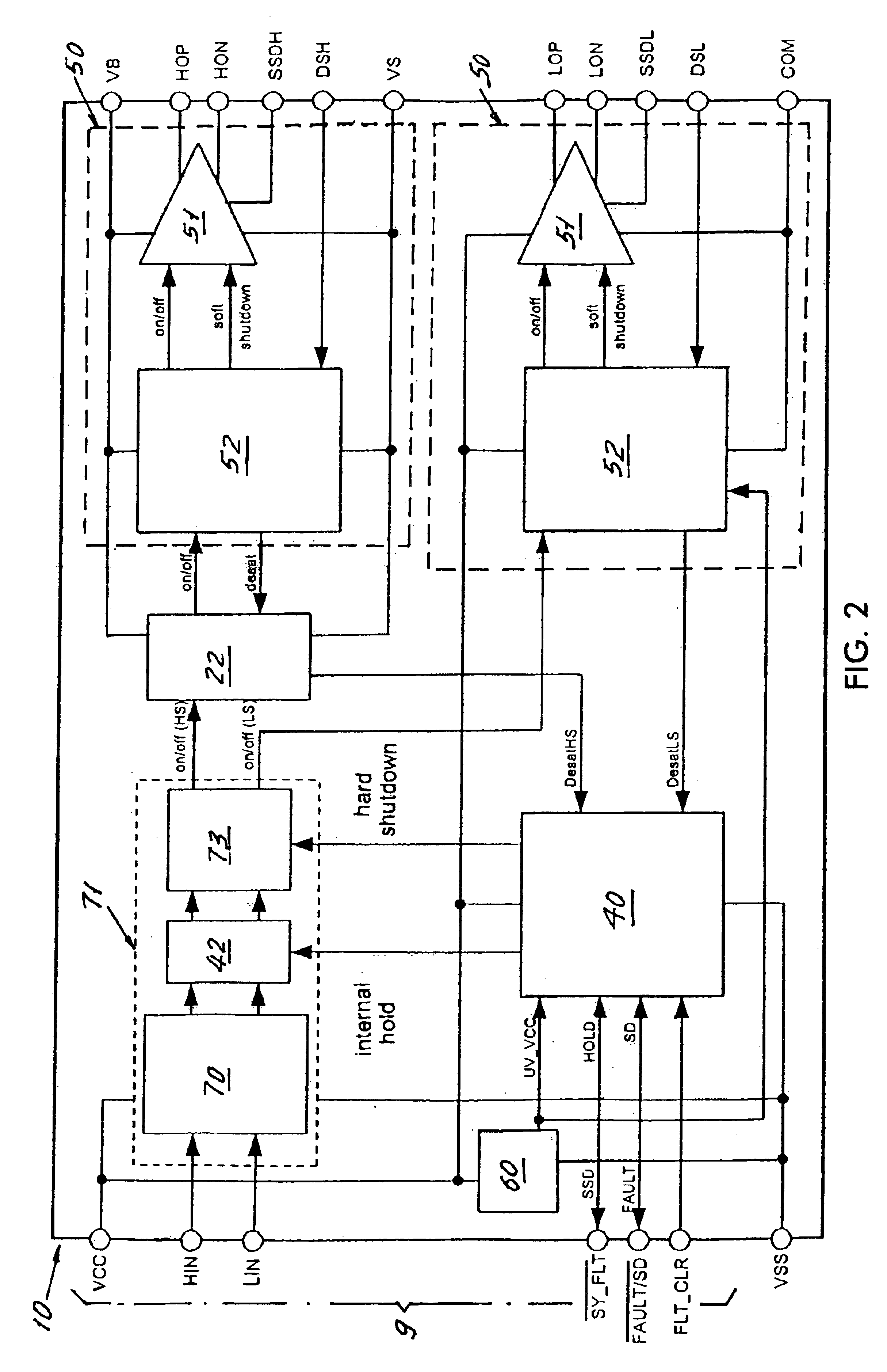
One embodiment of a gate driver integrated circuit 10 for driving and protecting an insulating gate bipolar transistor 110 comprises an input control stage 70, a hold logic stage 42, a switching logic stage 73, at least one gate driver output stage 50 and a fault control circuit 40. For example, the gate driver integrated circuit 10 has circuits integrated as shown in FIG. 2. The input control stage 70 is electrically connected to at least one external control input capable of connecting to an external controller. The input stage 70 has at least one control output to the hold logic circuit 42, which has at least one internal hold output and an internal connection to the fault control circuit 40 for activating a hold state (freeze), causing any changes in the signals from the input stage 70 to be ignored. The hold output is received by the switching logic stage 73, which has at least one switching output to each of the output stages 50 of the integrated circuit 10. The switching logi...


PUM


Abstract

A gate drive integrated circuit for switching power transistors using an external controller includes a gate driving capability and low quiescent current and allows use of a bootstrap supply technique for providing the logic supply voltage. The gate driver integrated circuit detects power transistor desaturation, protecting a desaturated transistor from transient over voltages by smoothly turning off the desaturated transistor via a soft shutdown sequence. A fault control circuit of the gate driver integrated circuit manages protection of supply under-voltage and transistor desaturation and is capable of communicating with a plurality of gate driver integrated circuits in a multi-phase system using a dedicated local network.

Description

BACKGROUND OF THE INVENTION1. Field of the InventionThe field of the invention is gate drivers for metal oxide silicon field effect transistors, especially gate drivers providing full protection and diagnostic feedback.2. Background of the InventionMetal oxide semiconductor field effect transistors (MOSFETs) have been used in power electronics applications for their ability to carry large currents and to block high off-state voltages, while having comparatively low on-state voltage drops across the transistor. Generally, there are two parasitic capacitances between the gate to source and the gate to drain that may cause switching delays if the gate driver does not support large initial currents.Conventional MOSFET gate driver circuits are simple, self-design circuits. More complex integrated circuit gate drivers are known that are controlled directly from transistor-transistor logic, complementary metal oxides semiconductors and microprocessor logic circuits. If the integrated drive...

Claims


Application Information

Patent Timeline
IPC IPC(8): H02M3/337H02M1/00H02M3/24H01L21/822H01L27/04H02M1/08H02M1/32H03K17/08H03K17/56
CPCH02M3/3376H02M1/32H03K17/163H03K17/168
Inventor GALLI, GIOVANNIGIANDALIA, MARCOMERELLO, ANDREA
Owner INFINEON TECH AMERICAS
Why Eureka
Try Eureka