
Microelectromechanical system optical sensor providing bit image data of a viewed image

a microelectromechanical system and optical sensor technology, applied in the field of optical microlens sun sensors, can solve the problems of consuming high power, lack of miniaturized low power attitude determination and control systems, and affecting the progress of space missions using nanosatellite constellations, etc., to achieve accurate interpolation, reduce power consumption, and reduce the effect of siz

Inactive Publication Date: 2005-03-01
THE AEROSPACE CORPORATION
View PDF2 Cites 39 Cited by
  • Summary
  • Abstract
  • Description
  • Claims
  • Application Information

AI Technical Summary

Benefits of technology

Still another object of the invention is to provide a compact sun sensor having a microlens for focusing collected sun light in a sensor housing having a reflective surface for folding an optical path onto an array of photosensitive diodes such as a pixelized array.
Still a further object of the invention is to provide a compact sun sensor having a microlens for focusing collected sun light in a sensor housing having a reflective surface for folding an optical path onto an array of photosensitive diodes as part of a readout chip for providing a bit image of the received sunlight.
The invention is directed to an integrated microelectro-mechanical system (MEMS) sun sensor having a microlens, a folded optical element, and an active pixel sensor array. When used in spinning spacecraft, the scanning sun sensor scans the sky during the rotation of the spacecraft to sweep out a two-dimensional intensity bitmap image of the sky. This image is divided into pixels in azimuth and elevation over the sensor field-of-view during one revolution of the spacecraft. This two-dimensional bit map offers additional information for accurately interpolating the position of the sun through data processing.
The advantages of this MEMS sun sensor includes lower power usage, smaller size, higher performance, and compatibility with planar semiconductor fabrication techniques. The sun sensor can be integrated as an ultra low power CMOS device with an on-board processor in a radiation tolerant hermetic package. Preferably, the MEMS sun sensor is micro-optical element used to form an image of the sun on the active pixel linear array formed by silicon micromachining MEMS techniques. The imaging pixels of the pixel array are formed in the integrated readout circuit. Folded optics are combined with analog and digital readout circuitry formed in an integrated circuit substrate. An integrated microcontroller provides sun sensor data processing and control, and spacecraft interfacing for communicating data. The sun sensor uses low power, has low-mass and low volume by integrating together the readout chip and the data processor chip as a critical spacecraft subsystem for effective use in nanosatellites and microsatellites, where spacecraft resources are at a premium. The power, weight and size savings of resources enable the use of multiple and redundant fault-tolerant sun sensor implementations on large spacecraft where more resources are available. The sun sensor is preferably fabricated using commercial CMOS processes and batch fabrication methods that benefit from mass production for reducing manufacturing costs. These and other advantages will become more apparent from the following detailed description of the preferred embodiment.

Problems solved by technology

Advanced space missions using nanosatellite constellations are hindered by a lack of miniaturized low power attitude determination and control systems.
However, these conventional sun sensors do not sweep the field-of-view for creating a two-dimensional bit map of the sky, which may enhance attitude determination with interpolations.
However, existing sun sensors are relatively large and consume high power.

Method used


Image

  • Microelectromechanical system optical sensor providing bit image data of a viewed image
  • Microelectromechanical system optical sensor providing bit image data of a viewed image
  • Microelectromechanical system optical sensor providing bit image data of a viewed image

Examples


Embodiment Construction

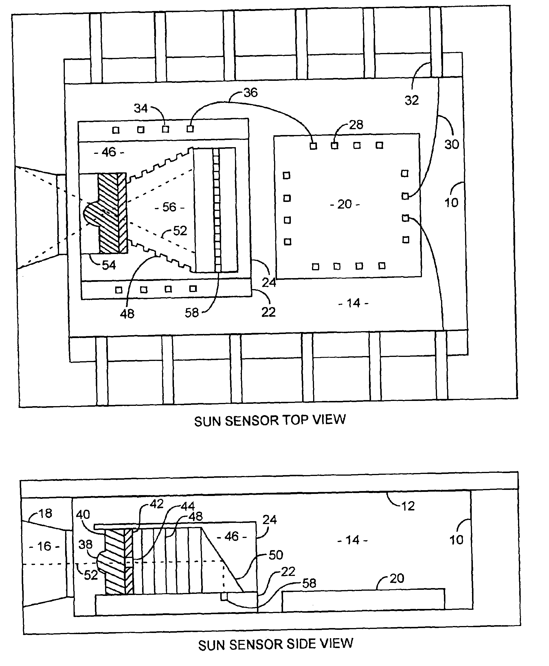
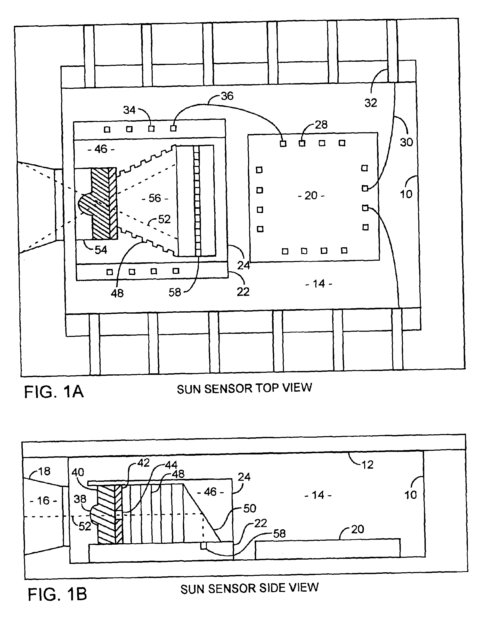
An embodiment of the invention is described with reference to the figures using reference designations as shown in the figures. Referring to FIGS. 1A and 1B, an integrated microelectro-mechanical system (MEMS) sun sensor is packaged using a ceramic package substrate 10 and a ceramic package lid 12 for forming a ceramic package cavity 14 that is hermetically sealed. The substrate 10 and lid 12 form a sun sensor package that can be mounted on a spinning spacecraft. The sun sensor package includes a front-end optical bandpass filter 16 disposed in a sun sensor viewing aperture 18 within the ceramic substrate 10. The filter 16 is an optically neutral density and band limiting filter.

A sun sensor data processor chip 20 is an integrated chip packaged with a sun sensor readout integrated chip 22. The readout chip 22 and the data processor chip 20 are bonded to the substrate 10 within the cavity 14. Sun sensor folded optics 24 are disposed on the sun sensor readout chip 22 that is bonded to...


PUM


Abstract

An integrated microelectromechanical system (MEMS) sun sensor includes a filter, microlens, aperture and a folded MEMS optical element combined with an active pixel sensor array to form an integrated spacecraft sun sensor in an integrated sealed package, offering lower power, smaller size and higher performance for use on spinning spacecraft useful in attitude determinations. Multiple like sun sensors can be disposed for increasing the reliability, spatial coverage or spatial resolution for a specific performance requirement.

Description

FIELD OF THE INVENTIONThe invention relates to the fields of optics and semiconductors. More particularly, the present invention relates to optical microlens sun sensors for sensing solar light.BACKGROUND OF THE INVENTIONAdvanced space missions using nanosatellite constellations are hindered by a lack of miniaturized low power attitude determination and control systems. Replacing large conventional spacecraft attitude sensors with smaller low power sun sensors is desirable for both three axis stabilized spacecraft and spinning spacecraft. A three axis stabilized spacecraft may have a centroid sun sensor having a central detector pointing at the sun with a series of circumferentially disposed detectors surrounding the central detector for determining when the sun is off center of a pointing line of sight when pointing directly towards the sun. An optical lens is used to focus the received sun light onto the central detector. A spinning spacecraft uses a scanning sun sensor that neces...

Claims


Application Information

Patent Timeline
IPC IPC(8): G01C21/24G01C21/02
CPCG01C21/24G01C21/02
Inventor OSBORN, JON V.
Owner THE AEROSPACE CORPORATION
Learn More