Unlock instant, AI-driven research and patent intelligence for your innovation.

Eeprom with split gate source side injection

a source side injection and gate source technology, applied in the field of semiconductor memory cells and arrays, can solve the problems of limiting the structure of column sectors, affecting the programming of erasers, and affecting so as to achieve the effect of increasing the level of erasers, high drain voltage requirements, and speed

Inactive Publication Date: 2005-03-01
SANDISK TECH LLC
View PDF99 Cites 17 Cited by
  • Summary
  • Abstract
  • Description
  • Claims
  • Application Information

AI Technical Summary

Benefits of technology

This patent describes a new type of memory cell that uses a small programming current to avoid common programming limitations. The cells are organized in sectors with each sector containing a single column or a group of columns. A high speed shift register is used to serially shift in data for the word lines, and a parallel loaded buffer register holds the data during the write operation. Additional speed is achieved by utilizing a parallel loaded buffer register and a verification process. The patent also describes a multi-bit memory cell that contains two bits per unit memory cell, coming from two floating gate portions, each having its own control gate. The programmed threshold voltage level of each floating gate must be limited in its upper value to be readable.

Problems solved by technology

In addition, the split gate structure is not susceptible to “overerase” related problems (a problem for single gate FLASH memories such as ETOX), and does not experience programming difficulty due to strong overerase, which can hinder programming after an erasure operation in split-gate CHE programming devices.
This erase approach poses some serious limitations.
This leads to the following disadvantages in the Ma implementation:(1) Limited to column sector architecture; i.e. cannot readily support the higher read performance row oriented sector architecture.

Method used


Image

  • Eeprom with split gate source side injection
  • Eeprom with split gate source side injection
  • Eeprom with split gate source side injection

Examples


second embodiment

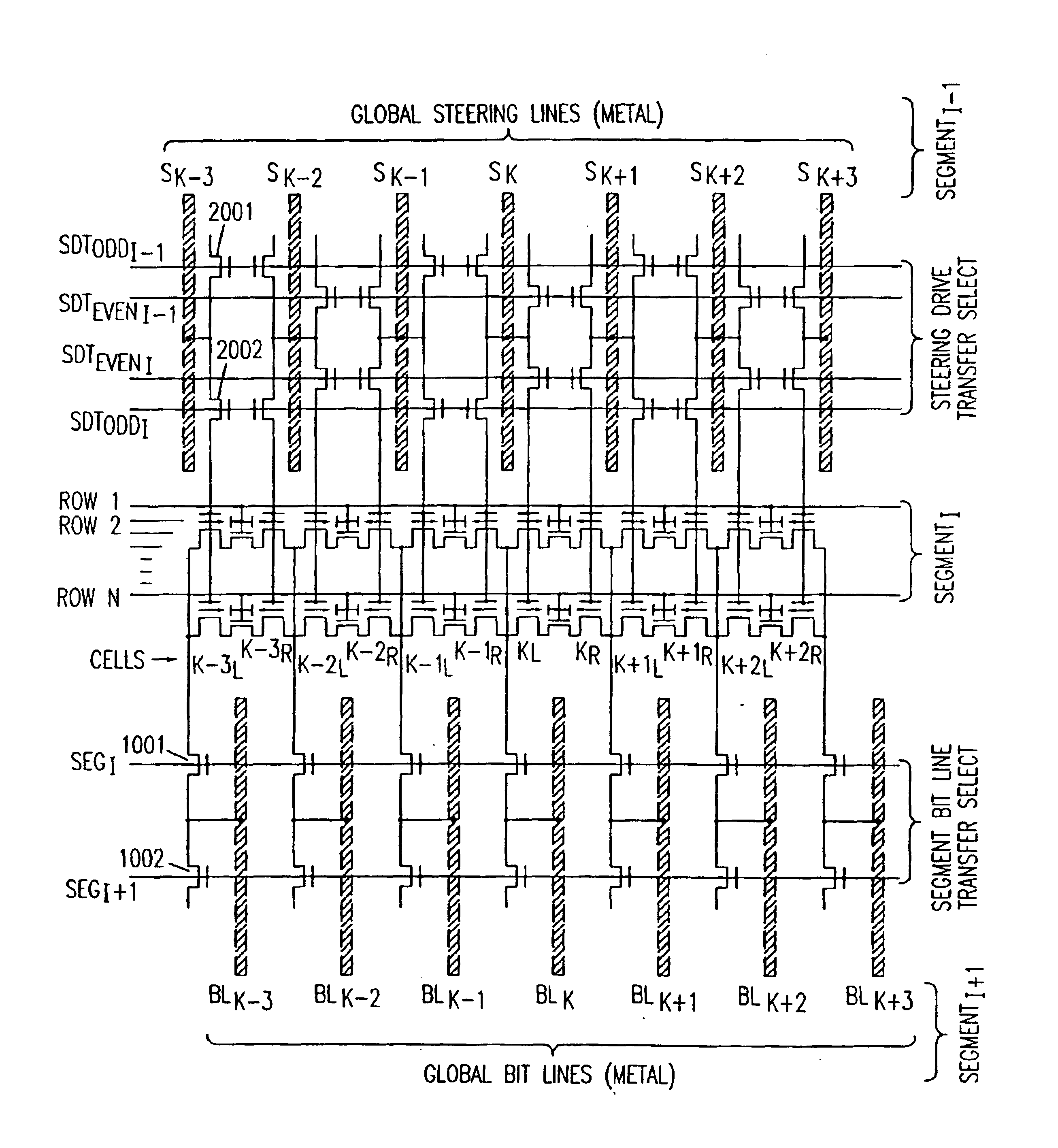
FIG. 5 is a two-poly embodiment in which programming occurs by taking drain 303 high, for example about 10V while raising control gate 308 just sufficiently so as to turn on select transistor 310. Since this VCG voltage can vary from one device to another it is possible to achieve the optimum injection conditions by keeping VCG at about 3V while raising source (virtual ground) 302 in a sawtooth fashion from about 0 to 3 volts and back to 0 again, with a period on the order approximately 1 microsecond.

This ensures that at some point along the sawtooth the optimum injection conditions are met. Reference can also be made to European Patent Application Serial No. 89312799.3 filed Aug. 12, 1989. To further enhance programming efficiency, in one embodiment a programming efficiency implant 330 (shown in dotted line) is introduced at the source side. To read the device, its source is 0V, drain is approximately 1.0 v and VCG approximately 4.5-5 v. To erase we employ poly 1-poly 2 tunneling b...

third embodiment

FIG. 6 is a cross-sectional view of alternative embodiment of a two poly cell, using source side injection for programming, aided by strong coupling to buried N+ drain 403, which acts also as a second control gate. Erase is by Fowler-Nordheim tunneling to channel 406 through a small thinned oxide region, formed for example to a thickness of about 100 Å, by utilizing a thin polyspacer. These process steps would be as follows: Once the drain oxide is formed (i.e. the oxide above drain 403), a first layer of poly, (approximately 2000 Å to 4000 Å thick) is deposited and a thin nitride dielectric is deposited on top. These layers are then etched using a poly 1 mask to delineate the lateral extent (as shown in FIG. 6) of the poly 1. A second layer of nitride is then deposited and anistropically etched back to underlying oxide, leaving the initial nitride layer on top of poly 1 plus nitride spacers along the poly 1 sidewalls. This protects the poly 1 sidewall from subsequent oxidation, all...


PUM


Abstract

Novel memory cells utilize source-side injection, allowing very small programming currents. If desired, to-be-programmed cells are programmed simultaneously while not requiring an unacceptably large programming current for any given programming operation. In one embodiment, memory arrays are organized in sectors with each sector being formed of a single column or a group of columns having their control gates connected in common. In one embodiment, a high speed shift register is used in place of a row decoder to serially shift in data for the word lines, with all data for each word line of a sector being contained in the shift register on completion of its serial loading. In one embodiment, speed is improved by utilizing a parallel loaded buffer register which receives parallel data from the high speed shift register and holds that data during the write operation, allowing the shift register to receive serial loaded data during the write operation for use in a subsequent write operation. In one embodiment, a verification is performed in parallel on all to-be-programmed cells in a column and the bit line current monitored. If all of the to-be-programmed cells have been properly programmed, the bit line current will be substantially zero. If bit line current is detected, another write operation is performed on all cells of the sector, and another verify operation is performed. This write / verify procedure is repeated until verification is successful, as detected or substantially zero, bit line current.

Description

TECHNICAL FIELDThis invention pertains to semiconductor memory cells and arrays, more particularly to electrically erasable programmable read only memories.BACKGROUNDErasable programmable read only memories (EPROMs) and electrically erasable programmable read only (EEPROMs) are well known in the art. These devices have the ability to store data in non-volatile fashion, while also being capable of being erased and rewritten as desired. EPROM devices are typically erased by exposing the integrated circuit device to ultraviolet radiation, while EEPROMs allow erasure to be performed electrically.One form of EEPROM device includes a so-called “split-gate” electrode, in which the control gate includes a first portion overlaying a floating gate and a second portion directly overlaying the channel. Such a split gate structure is described in a 5-Volt-Only Fast-Programmable Flash EEPROM Cell with a Double Polysilicon Split-Gate Structure by J. Van Houdt et al, Eleventh IEEE Non-Volatile Semi...

Claims


Application Information

Patent Timeline
Patent Type & Authority Patents(United States)
IPC IPC(8): G11C16/04H01L21/02H01L29/66H01L21/336H01L29/788G11C7/00G11C16/00H01L21/8247H01L29/76H01L31/107H01L33/00H10B69/00
CPCG11C16/0425H01L29/7881H01L27/115H01L27/11521G11C16/0491G11C16/0458H10B69/00H10B41/30
Inventor GUTERMAN, DANIEL C.SAMACHISA, GHEORGHEFONG, YUPIN KAWINGHARARI, ELIYAHOU
Owner SANDISK TECH LLC
Features
  • R&D
  • Intellectual Property
  • Life Sciences
  • Materials
  • Tech Scout
  • Unparalleled Data Quality
  • Higher Quality Content
  • 60% Fewer Hallucinations
Learn More