Light emitting device comprising light-emitting layer having triplet compound and light-emitting layer having singlet compound

a technology of light-emitting layer and compound, which is applied in the direction of discharge tube luminescnet screen, natural mineral layered product, other domestic articles, etc., can solve the problems of varying the lifetime of el element, degradation of luminous material, etc., and achieves the effect of improving the mobility of carriers, reducing operation voltage, and high light emission efficiency

Inactive Publication Date: 2005-03-08
SEMICON ENERGY LAB CO LTD
View PDF19 Cites 83 Cited by
  • Summary
  • Abstract
  • Description
  • Claims
  • Application Information

AI Technical Summary

Benefits of technology

The triplet compound has a higher light emission efficiency than the singlet compound and hence needs lower operation voltage (a voltage required to cause an EL element to emit light) in emitting light of the same luminance.
Furthermore, the present invention improves the mobility of carriers (electrons and holes) injected from an anode by providing a plurality of hole transporting layers between the anode and a

Problems solved by technology

Unfortunately, application of high voltage leads to degradation of the lumin

Method used


Image

  • Light emitting device comprising light-emitting layer having triplet compound and light-emitting layer having singlet compound
  • Light emitting device comprising light-emitting layer having triplet compound and light-emitting layer having singlet compound
  • Light emitting device comprising light-emitting layer having triplet compound and light-emitting layer having singlet compound

Examples


embodiment 1

[Embodiment 1]

In this embodiment, a description will be given of a method of manufacturing a pixel portion and a driving circuit provided at its periphery on the same insulator. However, for simplification of the description, with respect to the driving circuit, a CMOS circuit in which an n-channel transistor and a p-channel transistor are combined will be shown.

First, as shown in FIG. 3A, a glass substrate 201 is prepared as a insulator. In this embodiment, not-shown protection films (carbon films, specifically diamond-like carbon films) are provided on both surfaces (the front surface and the rear surface) of the glass substrate 201. As long as it is transparent to visible light, a material other than glass (for example, plastic) may be used.

Next, an base film 202 having a thickness of 300 nm is formed on the glass substrate 201. In this embodiment, as the base film 202, silicon oxynitride films are laminated and are used. At this time, it is appropriate that the concentration of ...

embodiment 2

[Embodiment 2]

This embodiment shows characteristics of EL elements having different EL layers that can be used in carrying out the present invention. Structures of the EL layers formed in this embodiment are shown in FIGS. 7A to 7D.

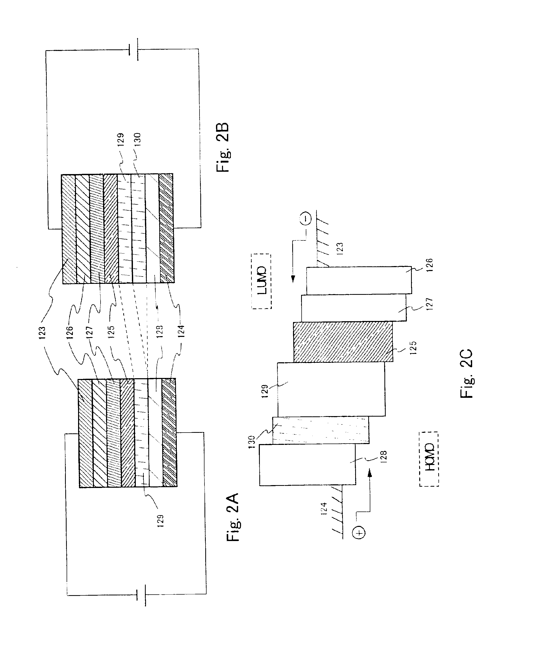
FIG. 7A shows the structure of an EL element a. First, a hole transporting layer is formed from α-NPD by evaporation to a thickness of 40 nm on an anode that is formed of a compound of indium oxide and tin oxide. On the hole transporting layer, a light emitting layer is formed from luminous materials consisting of Ir (ppy)3 and CBP (triplet compounds) by co-evaporation to a thickness of 20 nm. On the light emitting layer, a BCP layer with a thickness of 10 nm and a Alq3 layer with a thickness of 40 nm are formed by evaporation as an electron transporting layer. Then a cathode is formed from Yb to a thickness of 400 nm to complete the EL element a. Light emission from the EL element a utilizes triplet excitation energy by the triplet compounds.

FIG. 7B show...

embodiment 3

[Embodiment 3]

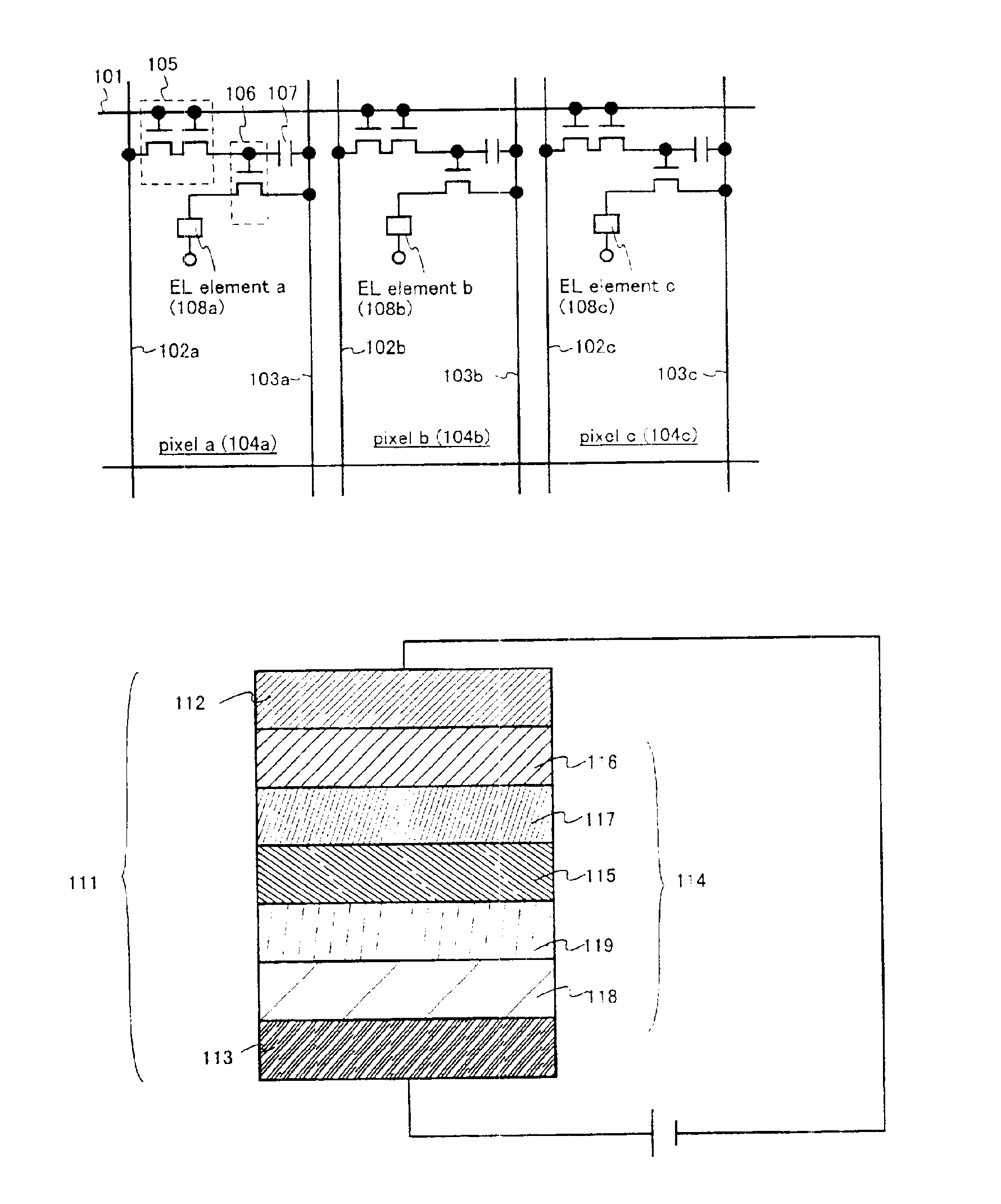
FIG. 12 shows a sectional structure of a pixel portion in an active matrix light emitting device of this embodiment. In FIG. 12, reference symbol 10 denotes an insulator, 11, the current controlling transistor (TFT) 604 of FIG. 5B. 12, a pixel electrode (anode), 13, a bank, and 14, a known hole injection layer. Reference symbols 15, 16, and 17 represent a light emitting layer that emits red light, a light emitting layer that emits green light, and a light emitting layer that emits blue light, respectively. Denoted by 18 is a known electron transporting layer, and 19, a cathode.

In this embodiment, triplet compounds are used for the red light emitting layer 15 and the blue light emitting layer 17 whereas a singlet compound is used for the green light emitting layer 16. In other words, an EL element that uses a singlet compound is an EL element that emits green light while EL elements that use triplet compounds are an EL element that emits red light and an EL element that...


PUM


Abstract

The luminance of different colors of light emitted from EL elements in a pixel portion of a light emitting device is equalized and the luminance of light emitted from the EL elements is raised. The pixel portion of the light emitting device has EL elements whose EL layers contain triplet compounds and EL elements whose EL layers contain singlet compounds in combination. The luminance of light emitted from the plural EL elements is thus equalized. Furthermore, a hole transporting layer has a laminate structure to thereby cause the EL elements to emit light of higher luminance.

Description

BACKGROUND OF THE INVENTION1. Field of the InventionThe present invention relates to a device having an element in which a luminous material is placed between electrodes (hereinafter referred to as light emitting element) (the device will hereafter be called a light emitting device). Specifically, the invention relates to a light emitting device having a light emitting element that employs as the luminous material an organic compound capable of providing EL (electro luminescence) (hereinafter referred to as EL element).2. Description of the Related ArtIn recent years, researches have been advanced on an EL element having a structure in which a thin film formed of an organic compound capable of providing EL (EL layer) is placed between an anode and a cathode, and light emitting devices utilizing the luminous characteristic of the EL element have been developed.An EL layer usually has a laminate structure typical example of which is one proposed by Tang et al. of Eastman Kodak Company...

Claims


Application Information

Patent Timeline
IPC IPC(8): H01L27/32H01L27/28H01L51/50H05B44/00
CPCH01L27/3211H01L27/3244H01L51/5012H01L51/5036H01L51/5016H01L27/3276H01L51/0059Y10S428/917H01L51/5048H01L51/56H01L2251/5315H01L2251/558H10K59/35H10K59/12H10K59/131H10K85/631H10K50/125H10K50/14H10K50/11H10K2101/10H10K2102/3026H10K2102/351H10K71/00
Inventor YAMAZAKI, SHUNPEINISHI, TAKESHIMIZUKAMI, MAYUMIIKEDA, HISAO
Owner SEMICON ENERGY LAB CO LTD
Why Eureka
Try Eureka