Field-effect transistor using a group III-V compound semiconductor

a compound semiconductor and field-effect transistor technology, applied in the direction of transistors, semiconductor devices, electrical equipment, etc., can solve the problems of complex element separation process, unsuitable for actual mass production, and inability to grow mixed crystals of group v, so as to achieve a lower composition ratio, lower composition ratio, and higher composition ratio of ga

Inactive Publication Date: 2005-03-15
FUJITSU LTD
View PDF7 Cites 4 Cited by
  • Summary
  • Abstract
  • Description
  • Claims
  • Application Information

AI Technical Summary

Benefits of technology

In another aspect of the above-described invention, the electron-supplying layer is composed of In1-yAlyAs, the first channel layer is composed of In1-xGaxAs, the second channel layer is composed of In1-x2Gax2As which has a lower composition ratio of In and a higher composition ratio of Ga than those in the first channel layer, and the buffer layer is composed of In1-yAlyAs. In this case, the second channel layer is composed of In1-x2Gax2As which has a lower composition ratio of In and a higher composition ratio of Ga than those in the first channel layer and the latt...

Problems solved by technology

However, a problem associated with such InP-type HEMT is that the drain resistance increases in current stress tests conducted at a high temperature.
The excess current caused by such impact ionization is observed as a drain conductance increase in the current-voltage characteristic of the HEMT and represents a serious problem from the standpoint of circuit design.
Generally, the compound semiconductor layer using...

Method used


Image

  • Field-effect transistor using a group III-V compound semiconductor
  • Field-effect transistor using a group III-V compound semiconductor
  • Field-effect transistor using a group III-V compound semiconductor

Examples


Embodiment Construction

The preferred embodiment of the present invention will be described below with reference to the drawings. However, the scope of protection of the present invention is not limited to the below-described embodiments and covers the invention described in the claims and equivalents thereof.

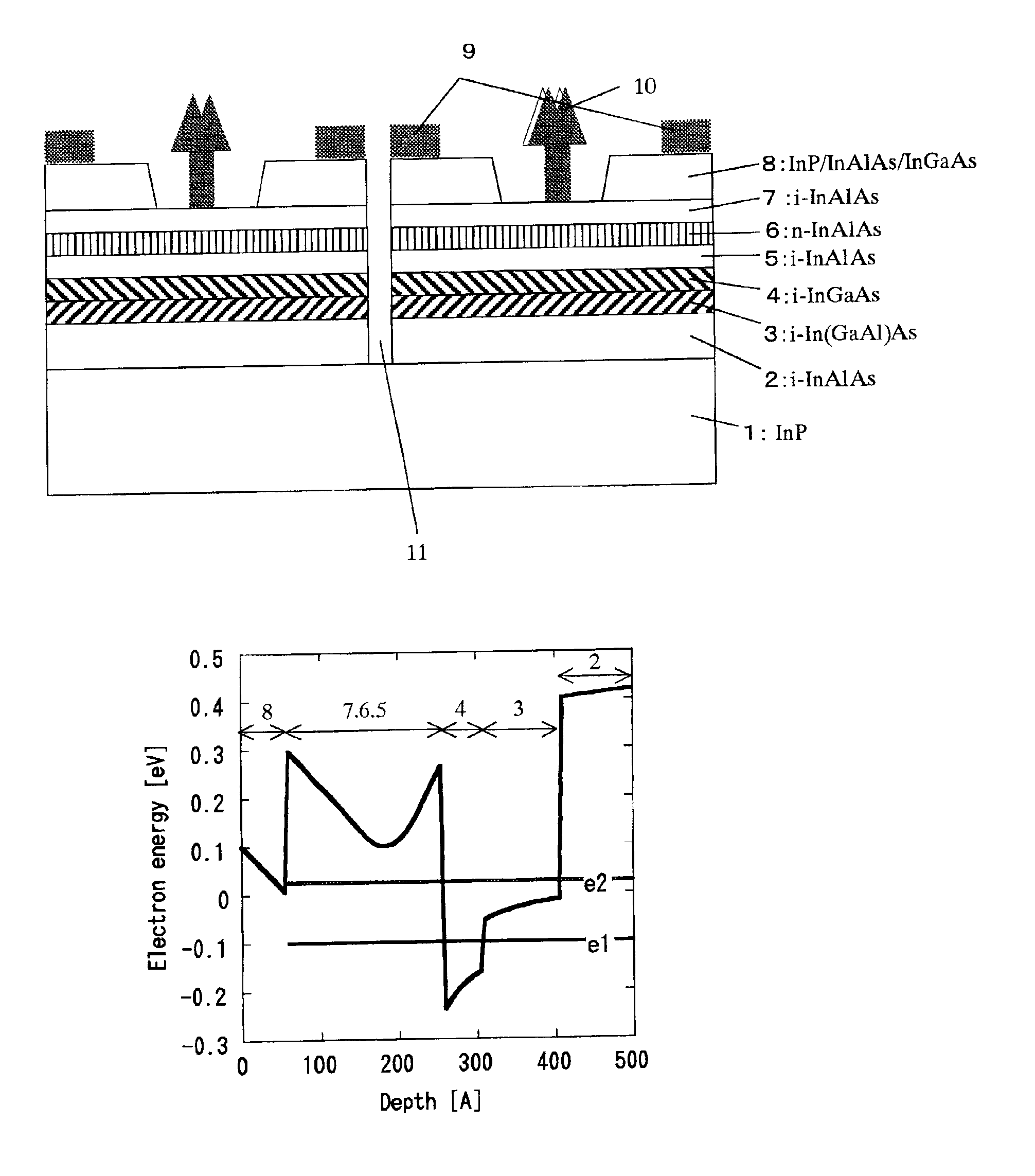
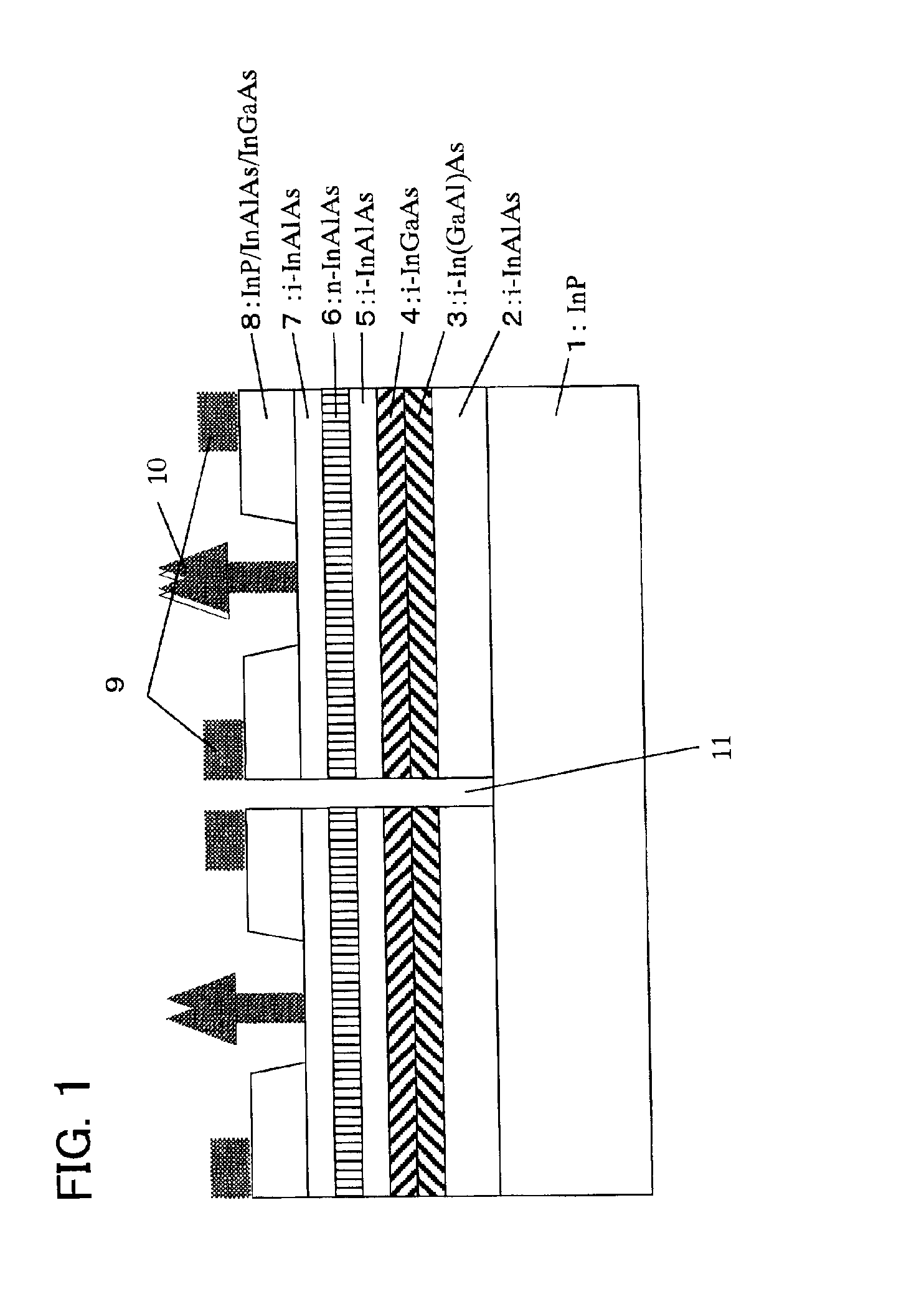
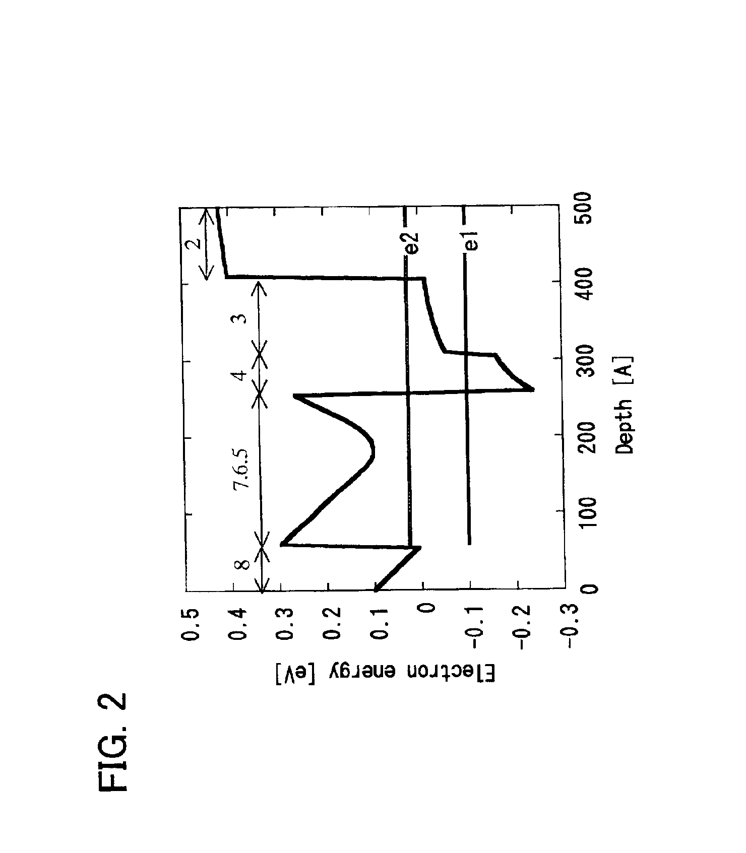
FIG. 1 shows a configuration of the HEMT of the present embodiment. In FIG. 1, two HEMTs are formed in parallel and an isolation groove 11 extending from the surface to the buffer layer 2 is formed therebetween. In the HEMT of this embodiment, an undoped (I type) In1-yAlyAs buffer layer 2 with a thickness, for example, of 200 nm, an undoped In1-x(Al1-zGaz)xAs second channel layer 3 with a thickness, for example, of 10 nm, an undoped In1-xGaxAs first channel layer 4 with a thickness, for example, of 5 nm, an undoped In1-yAlyAs spacer layer 5 with a thickness, for example, of 3 nm, an n-type In1-yAlyAs electron-supplying layer 6 doped with Si to 5×10¹⁸ / cm3 and having a thickness, for example, of 7 nm, a...


PUM


Abstract

A high electron mobility transistor using a Group III-V compound semiconductor comprises an undoped second channel layer laminated on an InP substrate via a buffer layer, an undoped first channel layer laminated on the second channel layer, and a doped electron-supplying layer laminated on the first channel layer. The first channel layer is composed of In1-xGaxAs and has an energy level of conduction band lower than that of the electron-supplying layer at the interface. The second channel layer is composed of a Group III-V compound semiconductor using a Group V element other than P, has an energy level of conduction band higher than that of the first channel layer, and has a band gap wider than that of the first channel layer.

Description

BACKGROUND OF THE INVENTION1. Field of the InventionThe present invention relates to a field-effect transistor using a Group III-V compound semiconductor, and more particularly to a high electron mobility transistor in which the impact ionization effect can be suppressed.2. Description of the Related ArtIn a high electron mobility transistor (HEMT) which is a field-effect transistor using a Group III-V compound semiconductor, an electron supply layer including a dopant is laminated with a channel layer containing no dopant, a two-dimensional electron gas is generated in the channel layer and the electrons flow in the channel layer containing no dopant so that a high-speed characteristic is obtained. Owing to this high-speed characteristic, the HEMTs have been widely used, for example, in amplifiers employed in communication systems.In the conventional HEMTs, it was suggested to employ an In1-xGaxAs layer as the channel layer where the electrons flow, thereby further improving perfor...

Claims


Application Information

Patent Timeline
IPC IPC(8): H01L27/06H01L29/812H01L21/338H01L29/10H01L29/778
CPCH01L27/0605H01L29/7783H01L29/1029
Inventor IMANISHI, KENJI
Owner FUJITSU LTD
Why Eureka
Try Eureka