

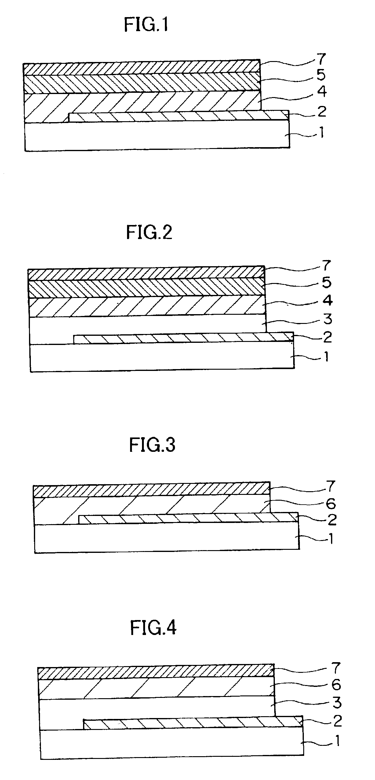
Organic electro-luminescent device
a technology of electroluminescent devices and organic materials, which is applied in the direction of discharge tubes/lamp details, natural mineral layered products, synthetic resin layered products, etc., can solve the problems of low probability of photon generation, high manufacturing cost, and insufficient brightness, and achieve excellent stability and durability, sufficient brightness, and formation in a large area
- Summary
- Abstract
- Description
- Claims
- Application Information
AI Technical Summary
Benefits of technology
Problems solved by technology
Method used
Image

Examples
synthesis example 1 (
Synthesis of Illustrative Compound (1))
To a 50 ml flask were added 1.74 g (10 mmol) of 1,10-decanediol and 30 ml of chlorobenzene, stirred, and dissolved. The solution of 2.64 g (10 mmol) of benzophenone-4,4′-diisocyanate dissolved in 10 ml of chlorobenzene was added dropwise to the flask over a period of 30 minutes and then heated and stirred at 150° C. for 2 hours under a stream of nitrogen. After the reaction was completed, the reaction solution was cooled to room temperature and added dropwise to 300 ml of methanol with stirring so that a polymer was allowed to precipitate. The resulting polymer was separated by filtration, thoroughly washed with methanol, and dried and then dissolved in 30 ml of tetrahydrofuran (THF). The solution was subjected to the re-precipitation step of adding dropwise to 300 ml of methanol three times, giving 3.8 g of an electron transporting polyurethane.
synthesis example 2 (
Synthesis of Illustrative Compound (7))
To a 50 ml flask were added 1.40 g (10 mmol) of 2,5-dihydroxy-1,4-benzoquinone and 30 ml of chlorobenzene, stirred, and dissolved. The solution of 1.62 ml (10 mmol) of hexamethylenediisocyanate dissolved in 10 ml of chlorobenzene was added dropwise to the flask over a period of 30 minutes and then heated and stirred at 150° C. for 2 hours under a stream of nitrogen. After the reaction was completed, the reaction solution was cooled to room temperature and added dropwise to 300 ml of methanol with stirring so that a polymer was allowed to precipitate. The resulting polymer was separated by filtration, thoroughly washed with methanol, and dried and then dissolved in 30 ml of tetrahydrofuran (THF). The solution was subjected to the re-precipitation step of adding dropwise to 300 ml of methanol three times, giving 2.4 g of an electron transporting polyurethane.
synthesis example 3 (
Synthesis of Illustrative Compound (24))
To a 50 ml flask were added 2.12 g (10 mmol) of 2,7-dihydroxy-9-fluorenone and 30 ml of chlorobenzene, stirred, and dissolved. The solution of 1.62 ml (10 mmol) of hexamethylenediisocyanate dissolved in 10 ml of chlorobenzene was added dropwise to the flask over a period of 30 minutes and then heated and stirred at 150° C. for 2 hours under a stream of nitrogen. After the reaction was completed, the reaction solution was cooled to room temperature and added dropwise to 300 ml of methanol with stirring so that a polymer was allowed to precipitate. The resulting polymer was separated by filtration, thoroughly washed with methanol, and dried and then dissolved in 30 ml of tetrahydrofuran (THF). The solution was subjected to the re-precipitation step of adding dropwise to 300 ml of methanol three times, giving 3.1 g of an electron transporting polyurethane.
PUM
| Property | Measurement | Unit |
|---|---|---|
| AC voltage | aaaaa | aaaaa |
| driving voltage | aaaaa | aaaaa |
| brightness | aaaaa | aaaaa |
Abstract
Description
Claims
Application Information