

Method of fabricating a light emitting device
a light emitting device and light technology, applied in the direction of semiconductor devices, electrical devices, transistors, etc., can solve the problems of low yield, inability to ensure reliability (the long life of the el element), and increased light emitting brightness of the el element, so as to reduce the manufacturing cost of an electric instrument and improve the yield of the light emitting device. , the effect of low manufacturing cos
- Summary
- Abstract
- Description
- Claims
- Application Information
AI Technical Summary
Benefits of technology
Problems solved by technology
Method used
Image

Examples
embodiment 1
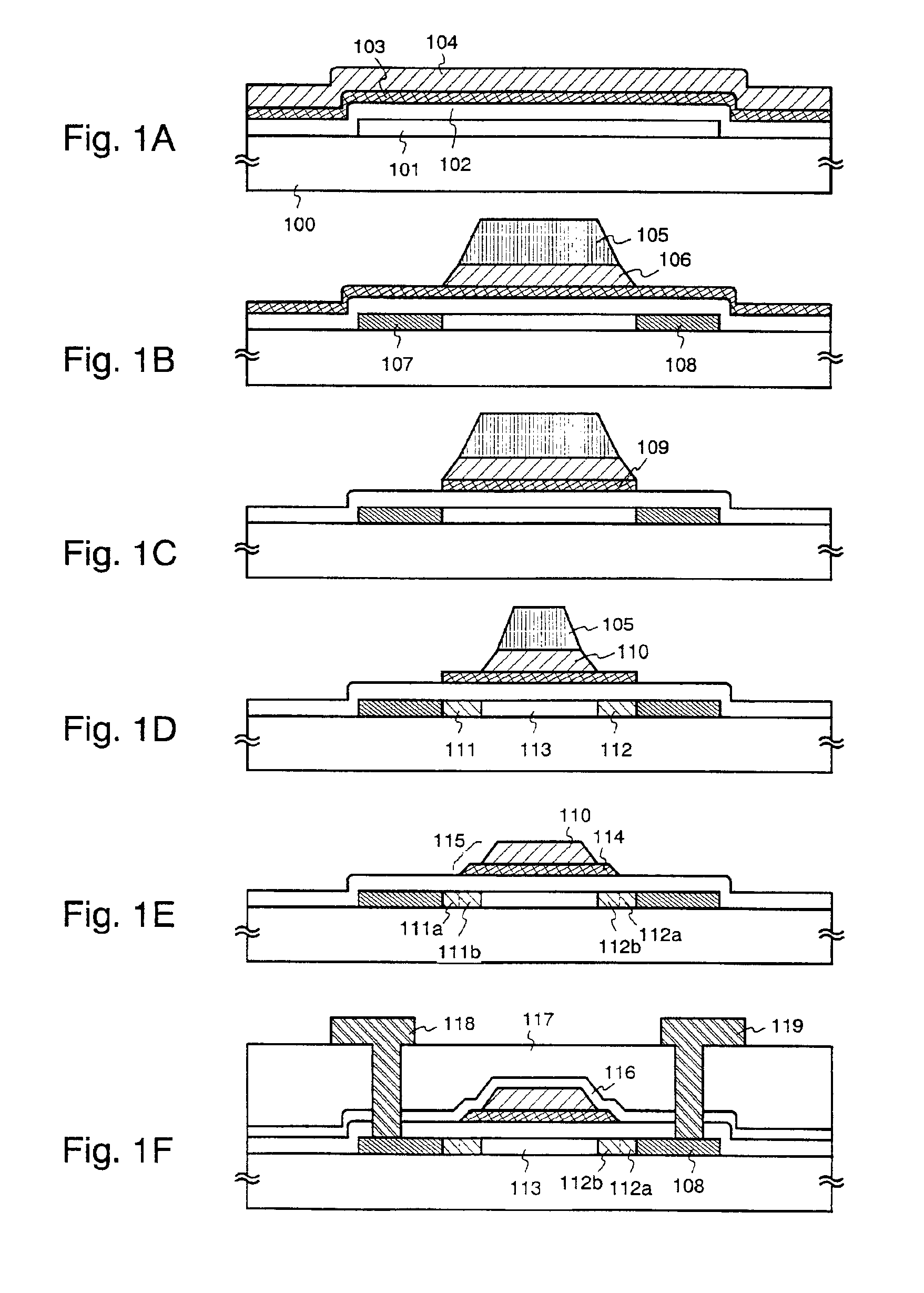
In this embodiment, a description will be given of a method of manufacturing a pixel portion and a driving circuit provided at its periphery on the same insulator. However, for simplification of the description, with respect to the driving circuit, a CMOS circuit in which an n-channel transistor and a p-channel transistor are combined will be shown.
First, as shown in FIG. 2A, a glass substrate 201 is prepared. In this embodiment, not-shown protection films (carbon films, specifically diamond-like carbon films) are provided on both surfaces (the front surface and the rear surface) of the glass substrate 201. As long as it is transparent to visible light, a material other than glass (for example, plastic) may be used.
Next, an under film 202 having a thickness of 300 nm is formed on the glass substrate 201. In this embodiment, as the under film 202, silicon nitride oxide films are laminated and are used. At this time, it is appropriate that the concentration of nitrogen of a layer adja...
embodiment 2
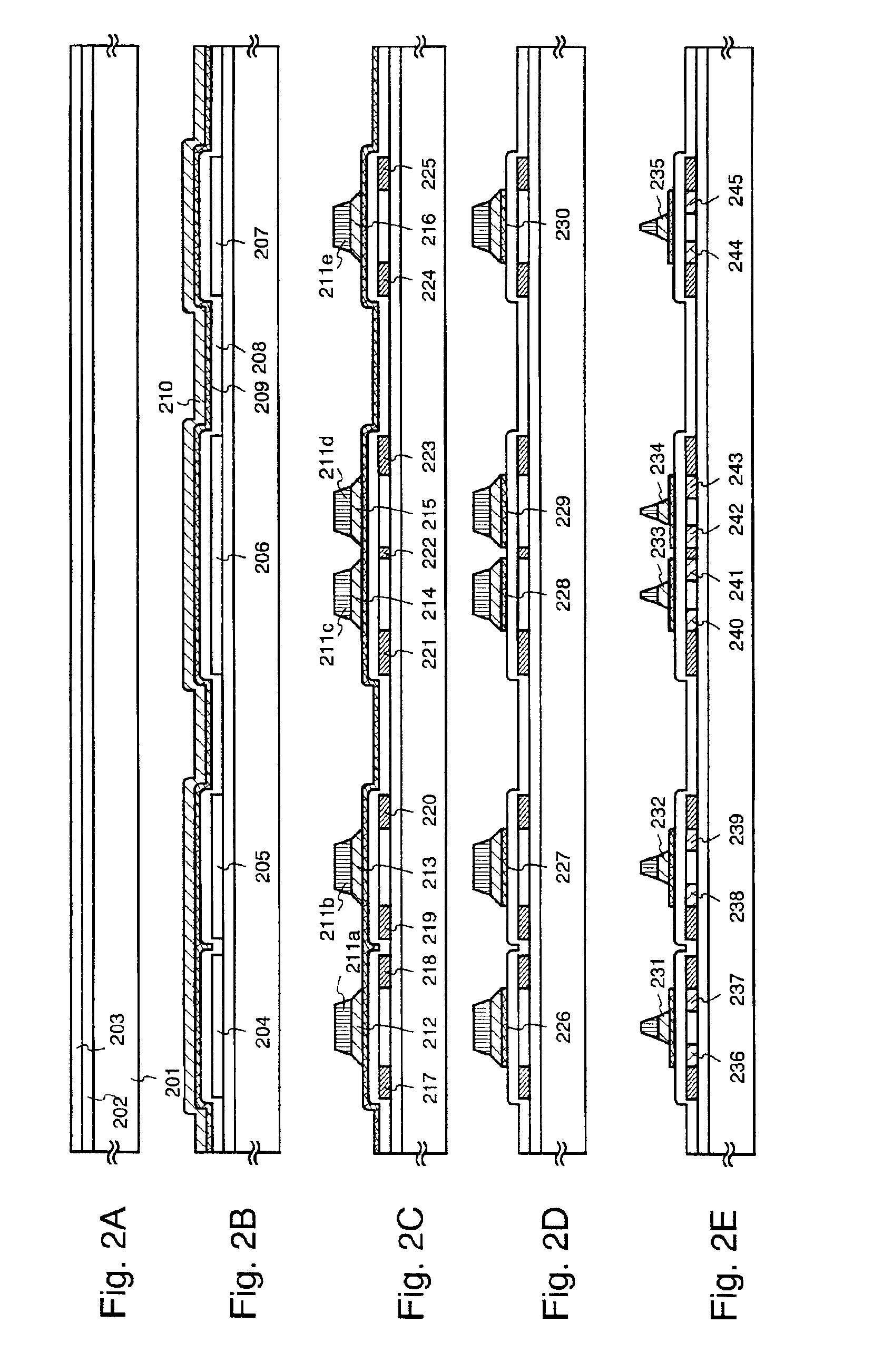
In this embodiment, an example in which an active matrix type light emitting device is fabricated by a fabricating process different from the embodiment 1 will be described. FIGS. 6A to 6D are used for the description.
First, in accordance with the fabricating process of the embodiment 1, steps up to FIG. 2C are performed. The state is shown in FIG. 6A. In this embodiment, a selection ratio of a first conductive film 209 and a second conductive film 210 is made smaller than the embodiment 1, and the second conductive film 210 is etched. In this case, in the etching step of FIG. 2C, it is appropriate that the flow of an oxygen gas is made 5.0×10⁻⁶ to 8.0×10⁻⁶ m3 / min.
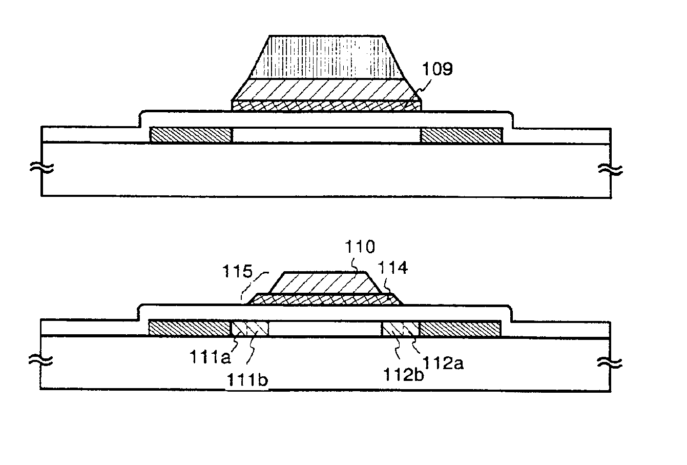
By doing so, in the first conductive film 209, portions which are not concealed by electrodes 212 to 216 made of the second conductive film are slightly etched and the film thickness is decreased. In this embodiment, an n-type impurity element (in this embodiment, phosphorus) is added in this state, and n-type impurity reg...
embodiment 3
In this embodiment, an example in which an active matrix type light emitting device is fabricated by a fabricating process different from the embodiment 1 will be described. FIGS. 7A to 7C are used for the description.
First, in accordance with the fabricating steps of the embodiment 1, steps up to FIG. 2C are performed. The state is shown in FIG. 7A. Next, in accordance with the etching condition of FIG. 2E of the embodiment 1, electrodes 212 to 216 made of a second conductive film are etched, and second gate electrodes 701 to 705 are formed (FIG. 7B).
Next, in this state, an n-type impurity element is again added under the same condition as FIG. 2E, and n-type impurity regions (b) 706 to 715 are formed.
Next, under the same etching condition as FIG. 3A, the first conductive film 209 is etched, and first gate electrodes 716 to 720 are formed. At this time, the n-type impurity region (b) 706 is divided into a region 706a not overlapping the first gate electrode 716 and a region 706b ov...
PUM
 Abstract
Description
Claims
Application Information