Method for removal of hemispherical grained silicon in a deep trench

a technology of hemispherical grained silicon and trenches, which is applied in the direction of electrical equipment, semiconductor devices, capacitors, etc., can solve the problems of deterioration of the etch stop layer between the hsg layer and the trench, inability to deploy hsg in the trench dram, and damage to the trench sidewall, etc., to achieve high selectivity, maintain or raise the capacitance per cell, no damage

Active Publication Date: 2005-03-29
CHANG LIAO HLDG
View PDF2 Cites 8 Cited by
  • Summary
  • Abstract
  • Description
  • Claims
  • Application Information

AI Technical Summary

Benefits of technology

The objective of the present invention is to provide a method for removal of the HSG layer in a deep trench but without damaging the trench sidewalls, as well as a method for maintaining or raising the capacitance per cell after incorporating HSG into trench DRAMs.
According to the aforementioned objective of the present invention, on the one hand, a method for removal of HSG layer by wet etching through a silicon germanium (SiGe) layer is provided. A potassium hydroxide (KOH) / propanone / water mixture is used as an etchant to recess the HSG layer. Once the buried SiGe layer is formed before the HSG layer, the HSG layer is successfully recessed and no damage is done to the trench sidewalls due to the high selectivity between the SiGe layer and the HSG layer by the etchant. Also the roughness of the trench sidewalls after removing the HSG layer is still acceptable for subsequent processes. The buried SiGe layer, moreover, decreases the BS resistance owing to its enhancement of the dopants activities in the buried strap (BS) region.
According to the aforementioned objective of the present invention, on the other hand, a buried SiGe layer formed before a HSG layer is served as an etch stop layer. The buried SiGe layer can be formed only on the collar region of the trench by implanting germanium atoms into the silicon trench with a predetermined angle. As a result, there is no etch stop layer between the trench and the HSG layer; the capacitance per cell can therefore be maintained or even raised. Furthermore, the etch stop layer can be formed selectively on the upper part of the trench, so other steps to remove that layer on the lower part of the trench are unnecessary, which effectively simplifies the technique to integrate HSG into current manufacturing processes of trench DRAMs.

Problems solved by technology

However, employing HSG in trench DRAMs is not feasible, because the physical property of HSG is quite similar to that of single crystalline silicon, which would cause inevitable damage of trench sidewalls while removing the upper part of the HSG layer in the deep trench by wet etching.
Unfortunately, any etch stop layer existing between the HSG layer and the trench would deteriorate capacitance enhancement due to the parasitic series capacitance thereof.
Nevertheless, the process is very complicated and therefore quite difficult.

Method used


Image

  • Method for removal of hemispherical grained silicon in a deep trench
  • Method for removal of hemispherical grained silicon in a deep trench
  • Method for removal of hemispherical grained silicon in a deep trench

Examples


Embodiment Construction

The embodiment in accordance with the present invention is disclosed in detail as following, when taken in conjunction with the accompanying drawings.

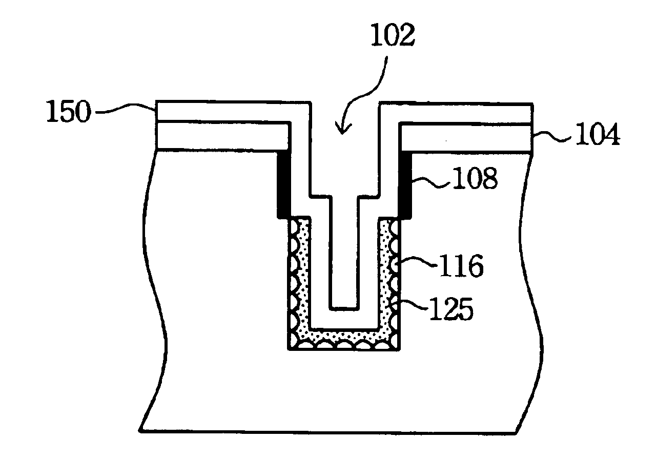
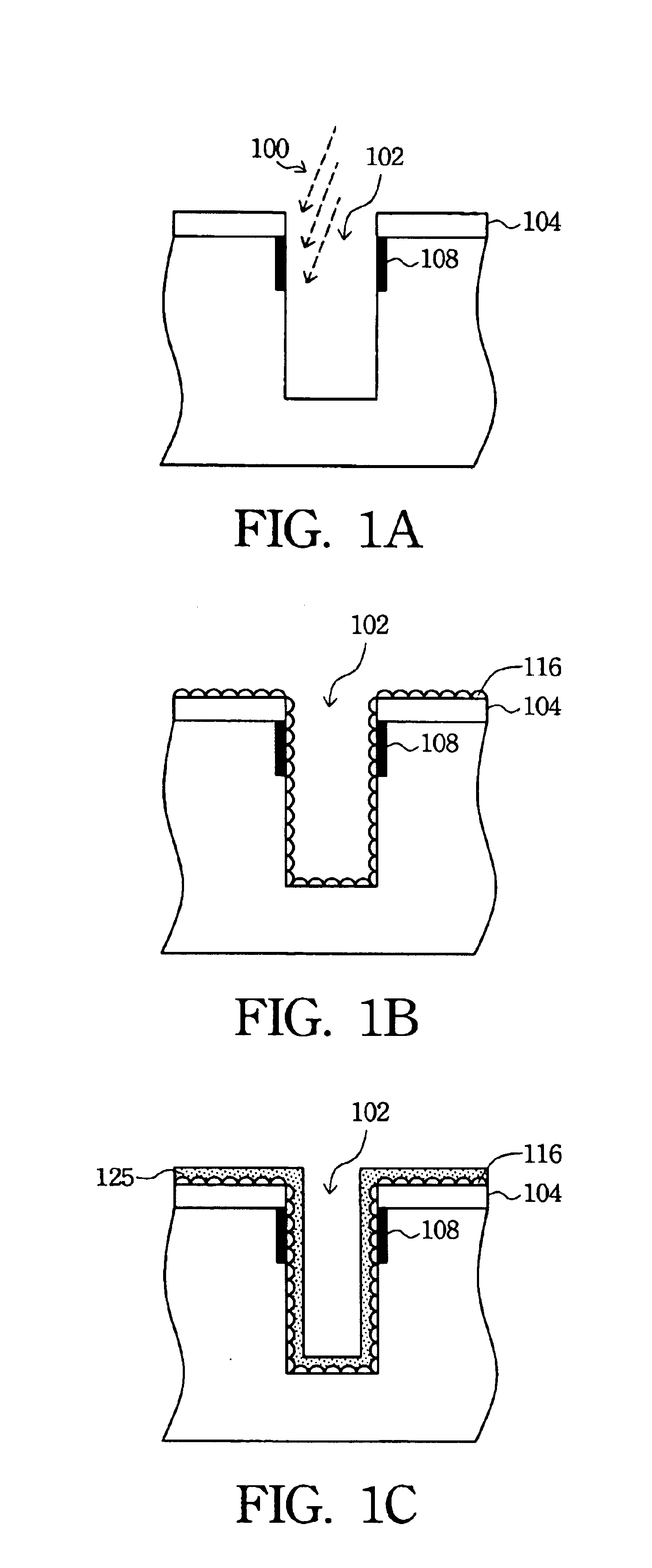
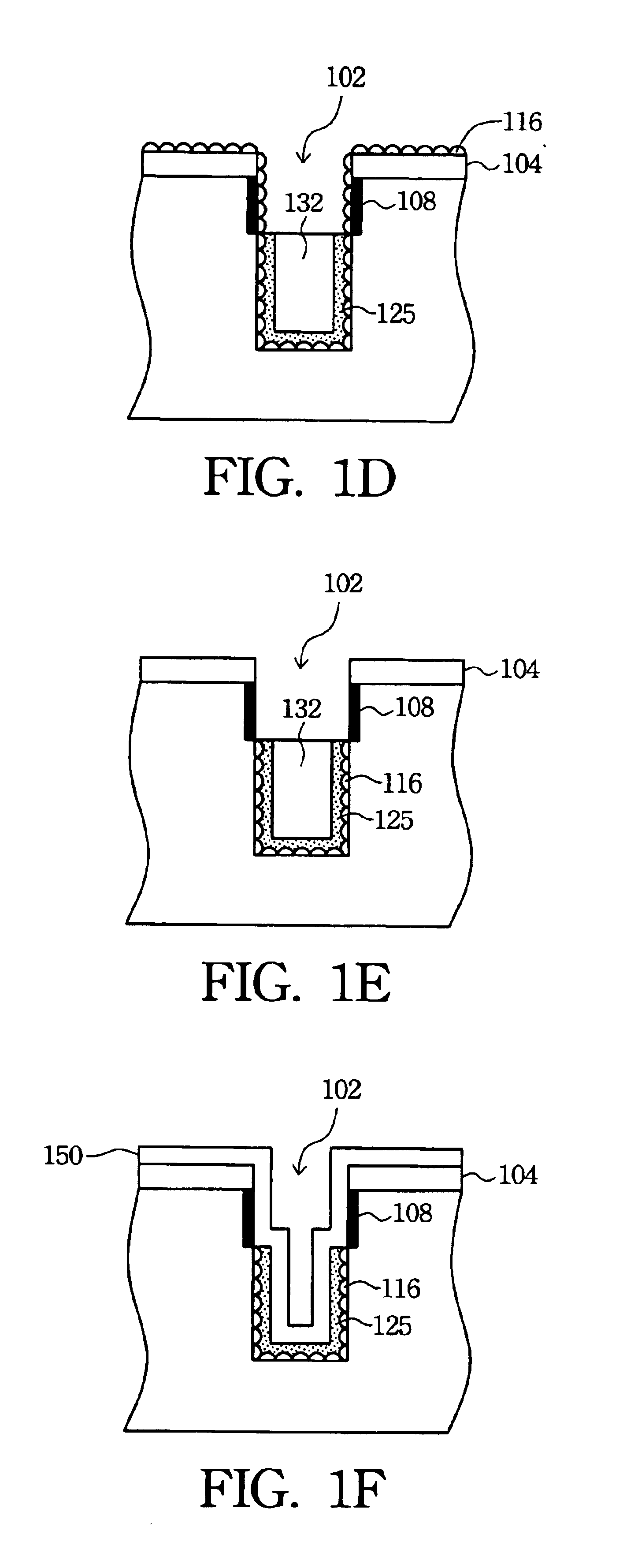
FIG. 1A illustrates a cross-sectional view of a substrate with a pad 104 and a trench 102 structure. A buried silicon germanium (SiGe) layer 108 is used as an etch stop layer. The buried SiGe layer 108 is formed in the collar region of the trench 102, as shown in FIG. 1A, by implanting 100 germanium atoms into the silicon trench 102 with a predetermined angle and followed by rapid thermal annealing. The predetermined angle is preferably from about 8 degrees to about 12 degrees, but most preferably is about 10 degrees. The SiGe layer 108 can be selectively formed on only the upper part of the trench 102 by controlling the implanting angle. Other steps to remove that layer on the lower part of the trench 102 are consequently unnecessary, which effectively simplifies the process. In addition, the buried SiGe layer 108 enhances activities ...


PUM


Abstract

A method for removal of hemispherical grained silicon (HSG) in a deep trench is described. A buried silicon germanium (SiGe) layer serving as an etch stop layer is formed in the collar region of the trench, followed by depositing a HSG layer. The HSG layer is then successfully striped by wet etching with a potassium hydroxide / propanone / water etchant, that is, without damage to the trench sidewalls, since a good etch rate selectivity between the HSG layer and the SiGe layer is obtained by the wet etchant. In addition, no etch stop layer exists between the HSG layer and the bottom of the trench when manufacturing trench capacitors in accordance with the method; capacitance degradation is therefore not of concern.

Description

FIELD OF THE INVENTIONThe present invention relates to a method for removal of hemispherical grained silicon, and more particularly, to a method for removal of hemispherical grained silicon in a deep trench through a silicon germanium (SiGe) etch stop layer.BACKGROUND OF THE INVENTIONRecently, the semiconductor industry has developed so rapidly that semiconductor devices almost extend into the sub-micron level. When either increasing integration density of a device or reducing its chip area, it becomes crucial to maintain an unchanged capacitance per cell especially for dynamic random access memory (DRAM) scaling. The lower limit for capacitances of storage capacitors is currently considered to be at least 25 fF.Increasing the surface area of a capacitor and implementing of high-k dielectrics would improve the performance of capacitance. A promising material, hemispherical grained silicon (HSG), has been extensively used to increase the surface area of a capacitor and also has been ...

Claims


Application Information

Patent Timeline
Patent Type & Authority Patents(United States)
IPC IPC(8): H01L21/02H01L21/311H01L21/3213H01L21/8242
CPCH01L21/31111H01L28/84H01L27/1087H01L21/32134H10B12/0387
Inventor WU, YUNG-HSIEN
Owner CHANG LIAO HLDG
Why Eureka
Try Eureka