High voltage N-LDMOS transistors having shallow trench isolation region

Inactive Publication Date: 2005-04-05
IBM CORP
View PDF20 Cites 82 Cited by
  • Summary
  • Abstract
  • Description
  • Claims
  • Application Information

AI Technical Summary

Benefits of technology

[0010]The manufacturing process shown above is advantageous when compared to conventional manufacturing processes because the invention forms the drain extension directly through the trench opening. Thus, a lower energy implant can be used than is used conventionally. Further, the penetration depth and unwanted diffusion is easily controlled because the implant is being made through the trench opening. In addition, the trench

Problems solved by technology

First, the method forms

Method used


Image

  • High voltage N-LDMOS transistors having shallow trench isolation region
  • High voltage N-LDMOS transistors having shallow trench isolation region
  • High voltage N-LDMOS transistors having shallow trench isolation region

Examples


Embodiment Construction

a partially completed LDMOS;

[0018]FIG. 7 is a schematic diagram of a partially completed LDMOS;

[0019]FIG. 8 is a schematic diagram of a partially completed LDMOS;

[0020]FIG. 9 is a schematic diagram of a partially completed LDMOS;

[0021]FIG. 10 is a schematic diagram of a partially completed LDMOS; and

[0022]FIG. 11 is a flowchart illustrating the embodiment of the invention.

DETAILED DESCRIPTION OF THE PREFERRED EMBODIMENT

[0023]Integration of microelectronics into consumer appliances, automotive, space technologies, etc., drives a market utilizing high performance CMOS (complementary metal oxide semiconductor), BJT's (bipolar junction transistors) and power MOS (metal oxide semiconductor) drivers. The lateral DMOS (LDMOS) transistor is typically chosen as the driving transistor, capable of switching high voltages.

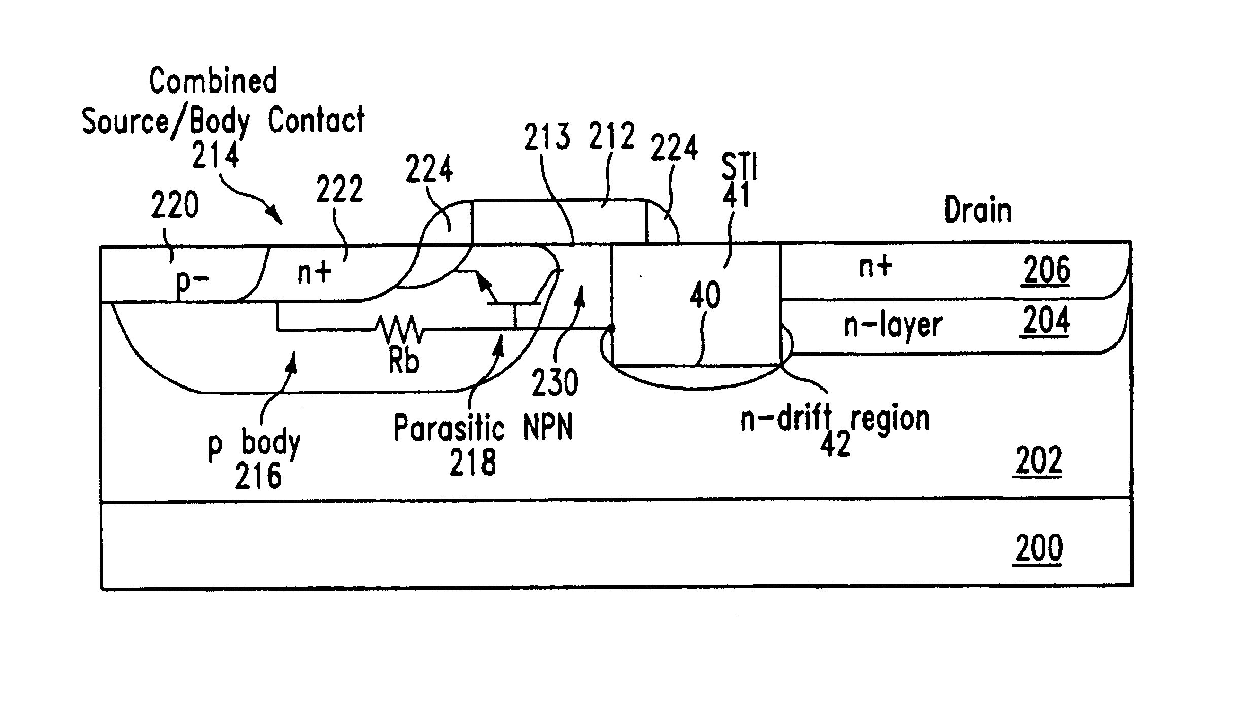
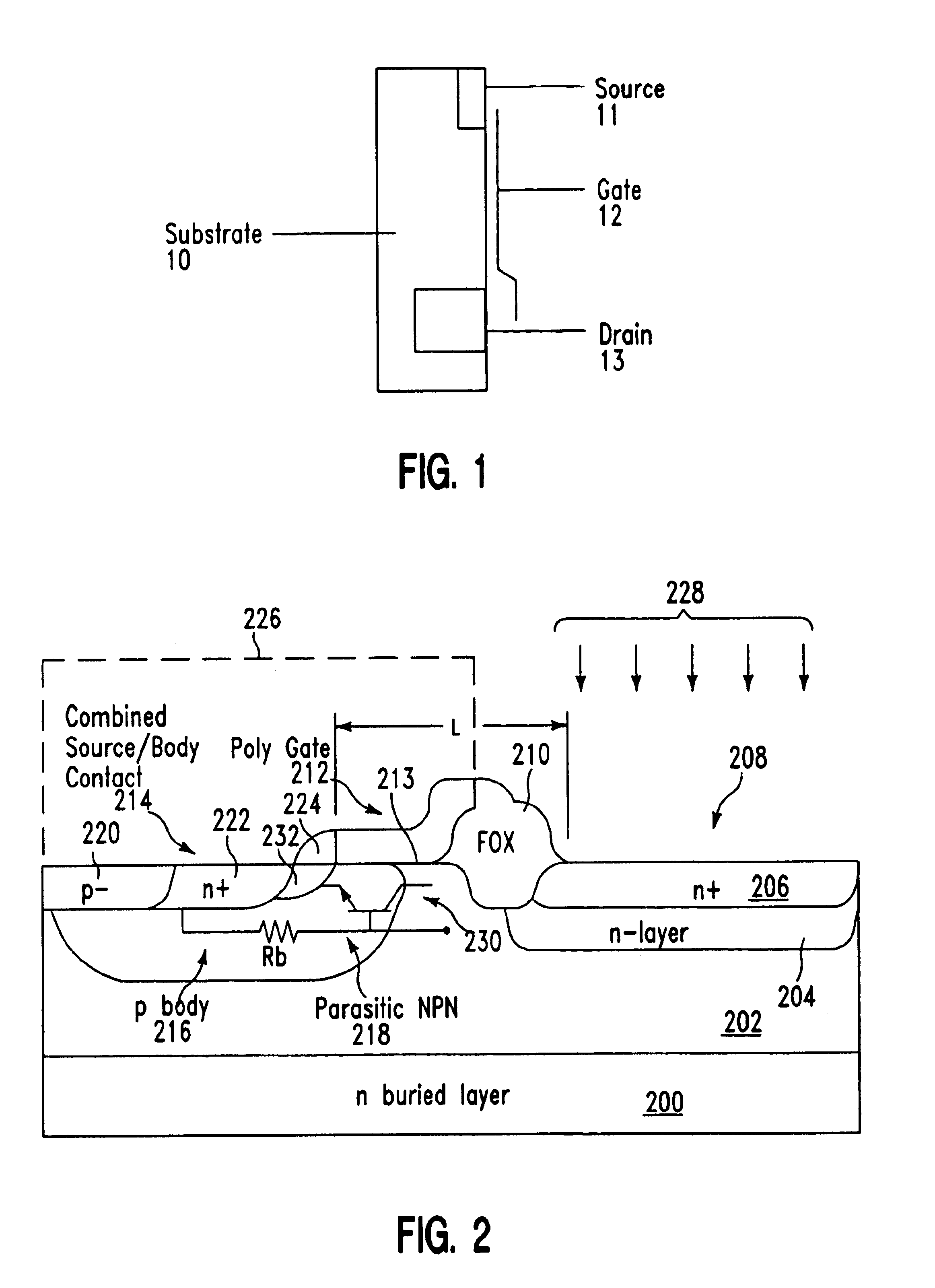
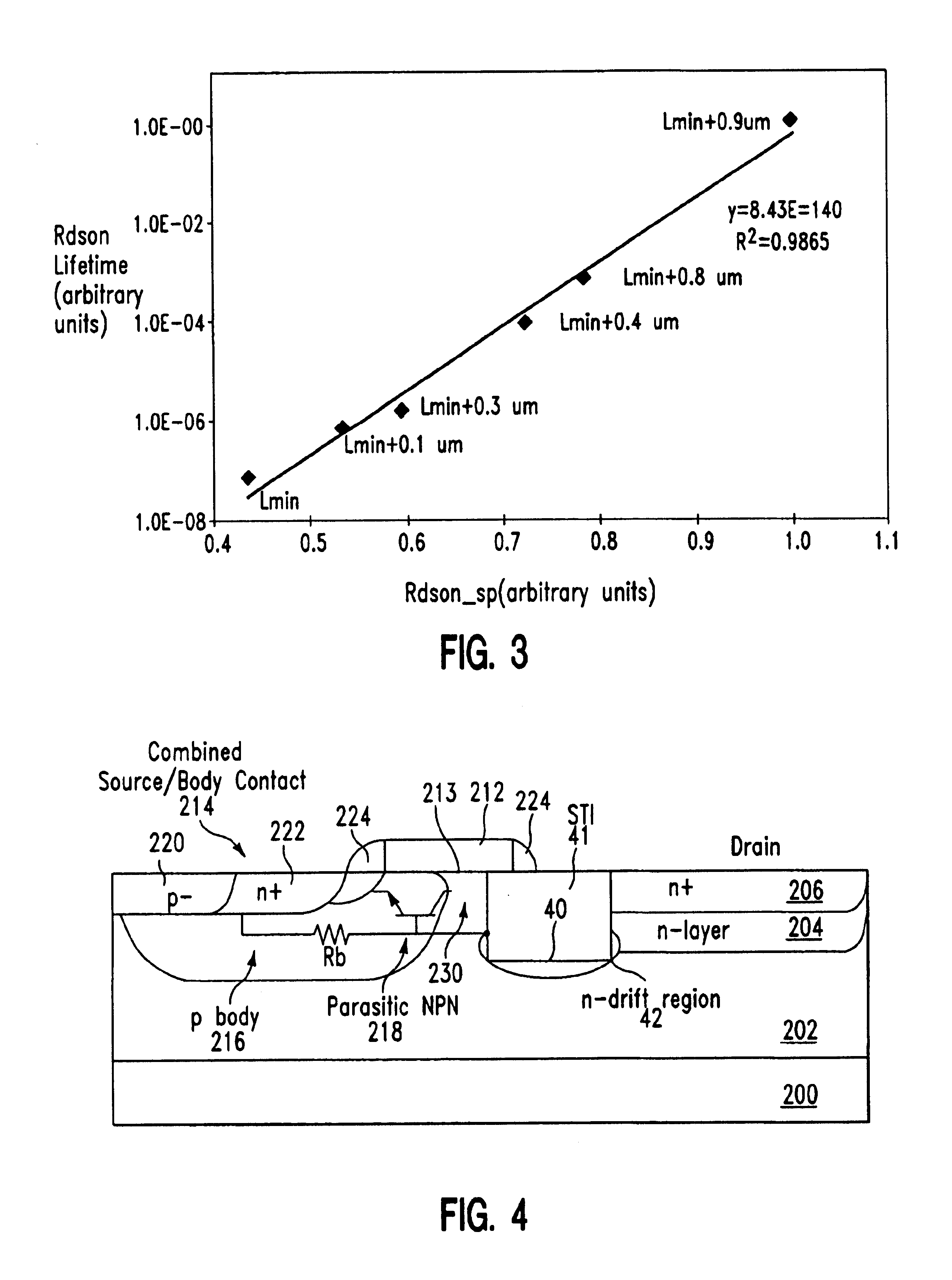
[0024]FIG. 1 illustrates a typical N-DMOS device schematic. The device includes a substrate 10, source 11, gate 12, and drain 13. In the device off state, the voltage of the d...


PUM


Abstract

A method and structure is disclosed for a transistor having a gate, a channel region below the gate, a source region on one side of the channel region, a drain region on an opposite side of the channel region from the source region, a shallow trench isolation (STI) region in the substrate between the drain region and the channel region, and a drain extension below the STI region. The drain extension is positioned along a bottom of the STI region and along a portion of sides of the STI. Portions of the drain extension along the bottom of the STI may comprise different dopant implants than the portions of the drain extensions along the sides of the STI. Portions of the drain extensions along sides of the STI extend from the bottom of the STI to a position partially up the sides of the STI. The STI region is below a portion of the gate. The drain extension provides a conductive path between the drain region and the channel region around a lower perimeter of the STI. The drain region is positioned further from the gate than the source region.

Description

BACKGROUND OF THE INVENTION[0002]1. Field of the Invention[0003]The present invention generally relates to transistors and more particularly to an improved N-type lateral double diffusion metal oxide semiconductor that has a shallow trench isolation region between the gate and the drain.[0004]2. Description of the Related Art[0005]Power semiconductor devices are currently being used in many applications. Such power devices include high-voltage integrated circuits, which typically include one or more high-voltage transistors, often on the same chip as low-voltage circuitry. A commonly used high-voltage component for these circuits is the lateral double diffused MOS transistor (LDMOS). LDMOS structures used in high-voltage integrated circuits may generally be fabricated using some of the same techniques used to fabricate the low voltage circuitry or logic circuitry. In general, these existing LDMOS structures are fabricated in a thick epitaxial layer of opposite conductivity type to t...

Claims


Application Information

Patent Timeline
IPC IPC(8): H01L29/66H01L21/02H01L29/78H01L21/336H01L21/265H01L29/08H01L29/423H01L29/02H01L29/40H01L29/06
CPCH01L29/0653H01L29/7816H01L29/0878H01L29/66689H01L21/26586H01L21/266H01L29/42368H01L29/086
Inventor ABADEER, WAGDI W.BROWN, JEFFREY S.GAUTHIER, JR., ROBERT J.RANKIN, JED H.TONTI, WILLIAM R.
Owner IBM CORP
Why Eureka
Try Eureka