Electroluminescence phosphor multilayer thin film and electroluminescence element

a technology of electroluminescence element and phosphor, which is applied in the direction of discharge tube/lamp details, luminescnet screen, transportation and packaging, etc., can solve the problems of insufficient light-emitting threshold voltage and luminance to be used in a practical el panel comprising an el element, and is substantially impossible to drive with commercially available ics at present. to achieve the effect of improving the efficiency of electron injection

Inactive Publication Date: 2005-04-05
IFIRE IP CORP
View PDF25 Cites 4 Cited by
  • Summary
  • Abstract
  • Description
  • Claims
  • Application Information

AI Technical Summary

Benefits of technology

These electron injection thin films further enhance the electron injection efficiency into the phosphor thin film. From this viewpoint, it will be more preferable if both of the electron injection thin films are provided.

Problems solved by technology

Therefore, in an EL element using an oxide type phosphor, an excessive load is exerted on IC for matrix-driving an actual EL panel, thus making it substantially impossible to be driven with commercially available ICs at present.
For achieving the above-mentioned object, the inventors studied characteristics of EL elements having Ga2O3:Eu thin films formed by conventional methods in detail and, as a result, have verified that these EL elements have a high emission threshold voltage of 260 V and a light-emitting luminance of about 80 cd / m2 at an application voltage of 300 V when driven at 1 kHz, thus being insufficient in terms of both light-emitting threshold voltage and luminance to be employed in a practical EL panel comprising an EL element.

Method used


Image

  • Electroluminescence phosphor multilayer thin film and electroluminescence element
  • Electroluminescence phosphor multilayer thin film and electroluminescence element
  • Electroluminescence phosphor multilayer thin film and electroluminescence element

Examples


first embodiment

FIG. 5 is a perspective view showing a major part of a first embodiment of the EL element in accordance with the present invention. This El element 101 comprises a substrate 2, and a lower electrode 3a, an insulating layer 4, a light-emitting layer 5, and an upper electrode 3b which are successively laminated on the substrate 2. An AC power supply is connected between the lower electrode 3a and upper electrode 3b.

Substrate 2

The material used as the substrate 2 preferably has a heat resistance temperature or melting point of at least 600° C., more preferably at least 700° C., further preferably at least 800° C., so as to be able to endure the temperature for forming individual layers constituting the EL element 101 and the temperature for annealing, which will be explained later, carried out at the time of forming the EL element.

The material is not restricted in particular as long as functional thin films such as the light-emitting layer 5 formed on the substrate 2 can be laminated ...

second embodiment

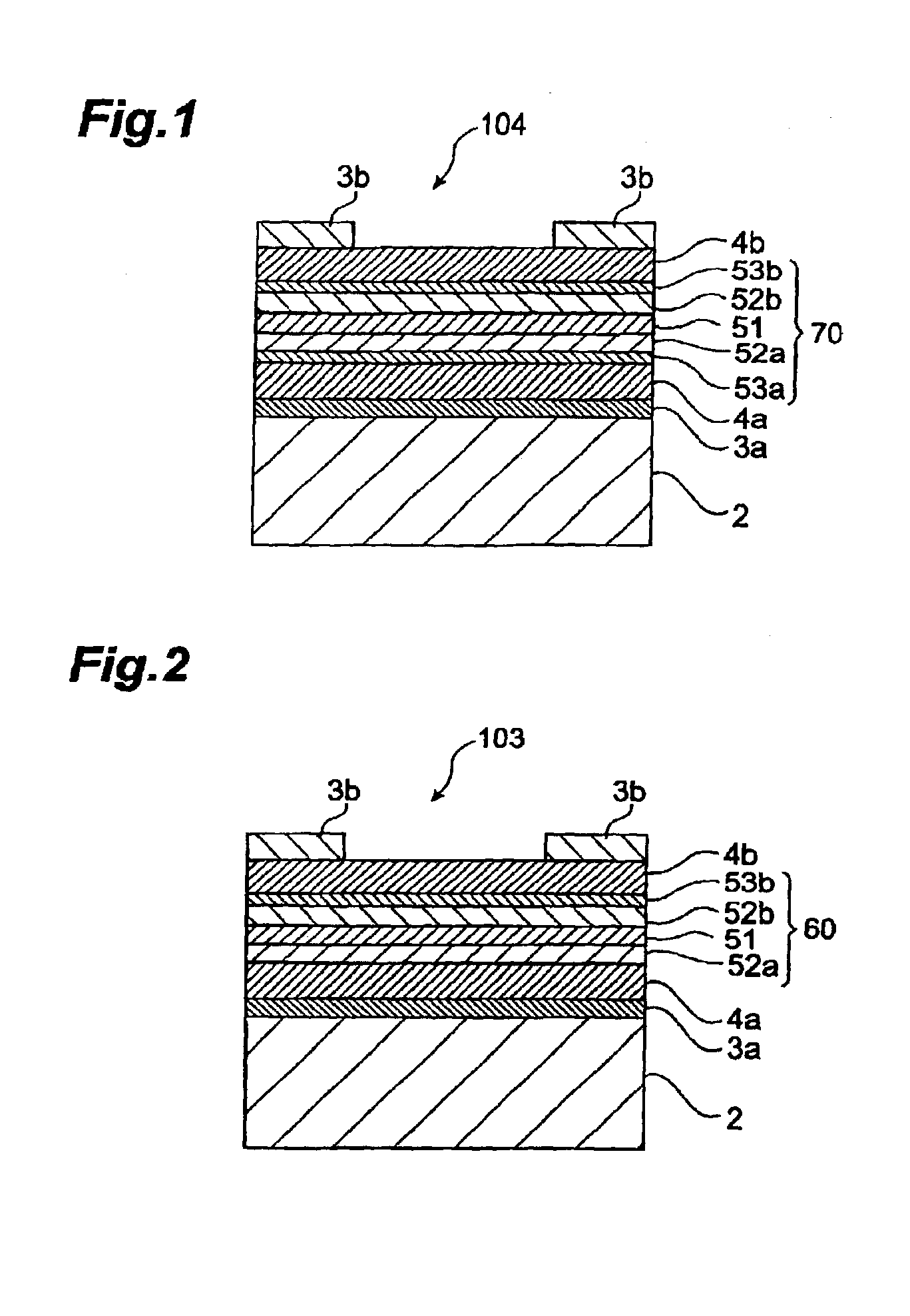
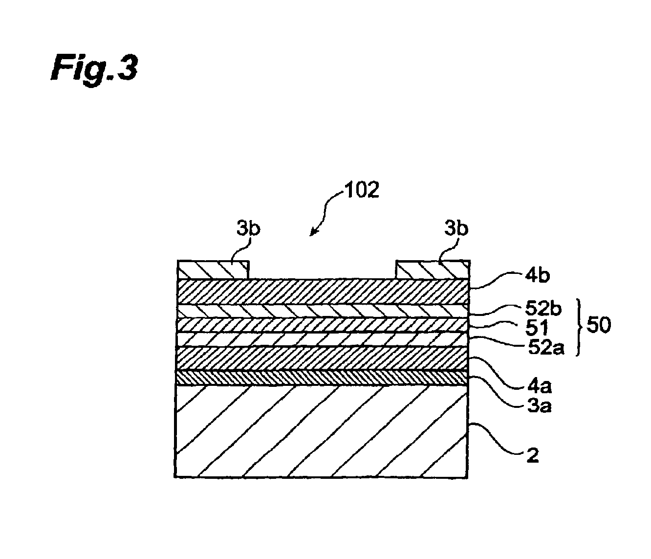
FIG. 3 is a sectional view showing a major part of a second embodiment of the EL element in accordance with the present invention. This EL element 102 comprises a substrate 2, and a lower electrode 3a, a lower insulating layer 4a, an EL phosphor multilayer thin film 50, an upper insulating layer 4b, and an upper electrode 3b which are successively laminated on the substrate 2. The EL phosphor multilayer thin film 50 comprises a lower buffer thin film 52a, a phosphor thin film 51, and an upper buffer thin film 52b which are successively laminated from the substrate 2 side.

Insulating Layers 4a, 4b

The lower insulating layer 4a can be obtained by the same material and forming method as with the insulating layer 4 constituting the EL element 101 shown in FIG. 5.

For the upper insulating layer 4b, on the other hand, a thin film insulating layer is preferably used. Examples of its material include silicon oxide (SiO2), silicon nitride (Si3N4), tantalum oxide (Ta2O5), strontium titanate (Sr...

third embodiment

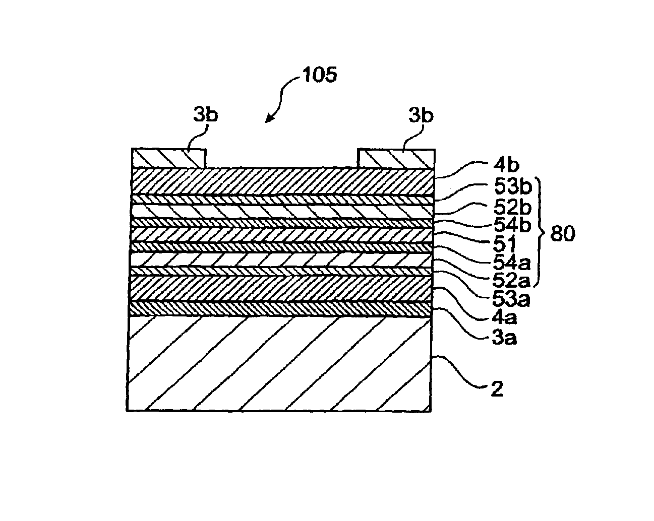
FIG. 2 is a sectional view showing a major part of a third embodiment of the EL element in accordance with the present invention. This EL element 103 is configured in the same manner as with the EL element 102 shown in FIG. 3 except that it comprises an EL phosphor multilayer thin film 60 instead of the EL phosphor multilayer thin film 50 The EL phosphor multilayer thin film 60 is configured in the same manner as with the EL phosphor multilayer thin film 50 except that an upper electron injection thin film 53b is further formed on the upper buffer thin film 52b.

The upper electron injection thin film 53b contains an oxide and / or a nitride. The upper electron injection thin film 53b functions as a layer for injecting electrons into the phosphor thin film 51, and can further improve the luminance when provided together with the buffer thin film 52b. The upper electron injection thin film 53b will be explained in detail in the following fourth embodiment.


PUM

PropertyMeasurementUnit
thicknessaaaaaaaaaa
thicknessaaaaaaaaaa
thicknessaaaaaaaaaa

Abstract

The present invention aims at realizing a phosphor thin film having a high luminance with a low emission threshold voltage, and an EL element comprising the same. The EL element of the present invention comprises a substrate, and a lower electrode, a lower buffer thin film containing a sulfide such as ZnS, a phosphor thin film containing an oxide such as a gallate as a matrix material, an upper buffer thin film containing a sulfide such as ZnS, and an upper electrode which are successively laminated on the substrate.

Description

BACKGROUND OF THE INVENTION1. Field of the InventionThe present invention relates to an EL (electroluminescence) element and an EL phosphor used therefor, a thin film multilayer structure of an oxide EL phosphor in particular.2. Related Background ArtIn recent years, studies of thin film EL elements as large-size, lightweight flat display panels have been actively under way. FIG. 6 is a perspective view schematically showing an example of conventional EL display. This EL element 100 is a monochromatic EL display comprising a phosphor thin film made of yellowish-orange-emitting, manganese-doped zinc sulfide (ZnS:Mn) disposed between two thin film insulating layers. It has a so-called double insulating structure and has already been in actual use.Specifically, a lower electrode 13a having a predetermined pattern is formed on a substrate 12 made of glass, whereas a dielectric thin film is formed as a lower insulating layer 14a on the lower electrode 13a. A light-emitting layer 15 made ...

Claims


Application Information

Patent Timeline
Patent Type & Authority Patents(United States)
IPC IPC(8): C09K11/77H05B33/14H05B33/20H05B33/12
CPCC09K11/7729H05B33/20H05B33/14Y10T428/31504
Inventor YANO, YOSHIHIKOTAKAHASHI, MASAKIOIKE, TOMOYUKIKATAOKA, NARUKI
Owner IFIRE IP CORP
Why Eureka
Try Eureka